PCA9555 All information provided in this document is subject to legal disclaimers. © NXP Semiconductors N.V. 2017. All rights reserved.
Product data sheet Rev. 10 — 8 November 2017 7 of 34
NXP Semiconductors
PCA9555
16-bit I
2
C-bus and SMBus I/O port with interrupt
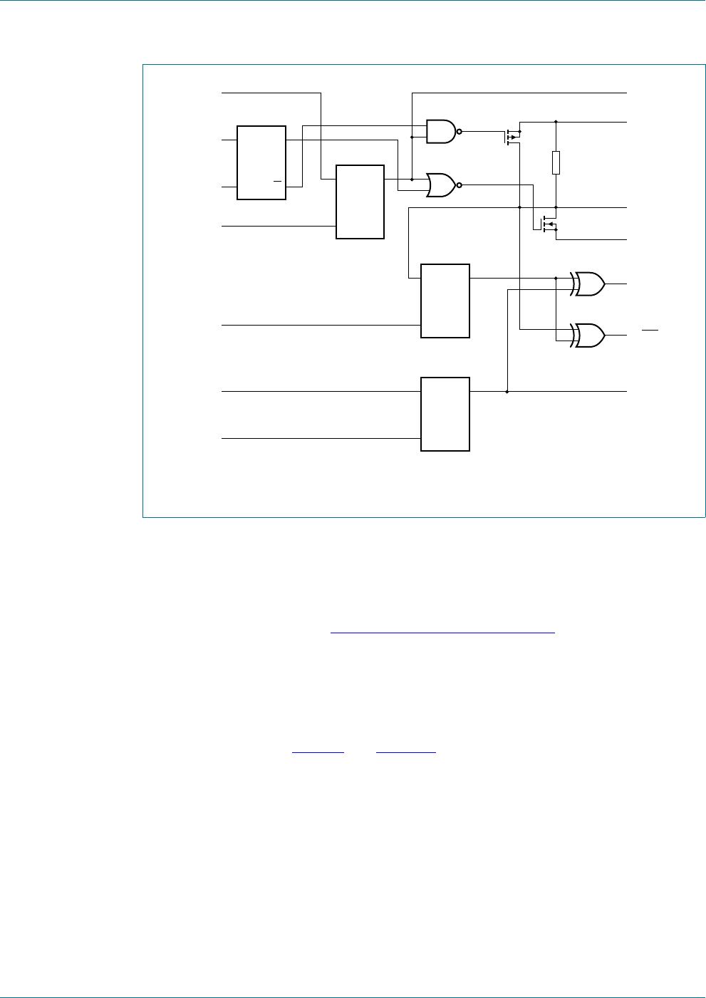
6.2.2 Registers 0 and 1: Input port registers
This register is an input-only port. It reflects the incoming logic levels of the pins,
regardless of whether the pin is defined as an input or an output by Register 3. Writes to
this register have no effect.
The default value ‘X’ is determined by the externally applied logic level.
6.2.3 Registers 2 and 3: Output port registers
This register is an output-only port. It reflects the outgoing logic levels of the pins defined
as outputs by Registers 6 and 7. Bit values in this register have no effect on pins defined
as inputs. In turn, reads from this register reflect the value that is in the flip-flop controlling
the output selection, not the actual pin value.
6.2.4 Registers 4 and 5: Polarity Inversion registers
This register allows the user to invert the polarity of the Input port register data. If a bit in
this register is set (written with ‘1’), the Input port data polarity is inverted. If a bit in this
register is cleared (written with a ‘0’), the Input port data polarity is retained.
Table 5. Input port 0 Register
Bit 7 6 5 4 3 2 1 0
Symbol I0.7 I0.6 I0.5 I0.4 I0.3 I0.2 I0.1 I0.0
Default XXXXXXXX
Table 6. Input port 1 register
Bit 7 6 5 4 3 2 1 0
Symbol I1.7 I1.6 I1.5 I1.4 I1.3 I1.2 I1.1 I1.0
Default XXXXXXXX
Table 7. Output port 0 register
Bit 7 6 5 4 3 2 1 0
Symbol O0.7 O0.6 O0.5 O0.4 O0.3 O0.2 O0.1 O0.0
Default 11111111
Table 8. Output port 1 register
Bit 7 6 5 4 3 2 1 0
Symbol O1.7 O1.6 O1.5 O1.4 O1.3 O1.2 O1.1 O1.0
Default 11111111
Table 9. Polarity Inversion port 0 register
Bit 7 6 5 4 3 2 1 0
Symbol N0.7 N0.6 N0.5 N0.4 N0.3 N0.2 N0.1 N0.0
Default 00000000
Table 10. Polarity Inversion port 1 register
Bit 7 6 5 4 3 2 1 0
Symbol N1.7 N1.6 N1.5 N1.4 N1.3 N1.2 N1.1 N1.0
Default 00000000