CY7C024E, CY7C0241E
CY7C025E, CY7C0251E
Document Number: 001-62932 Rev. *A Page 11 of 22
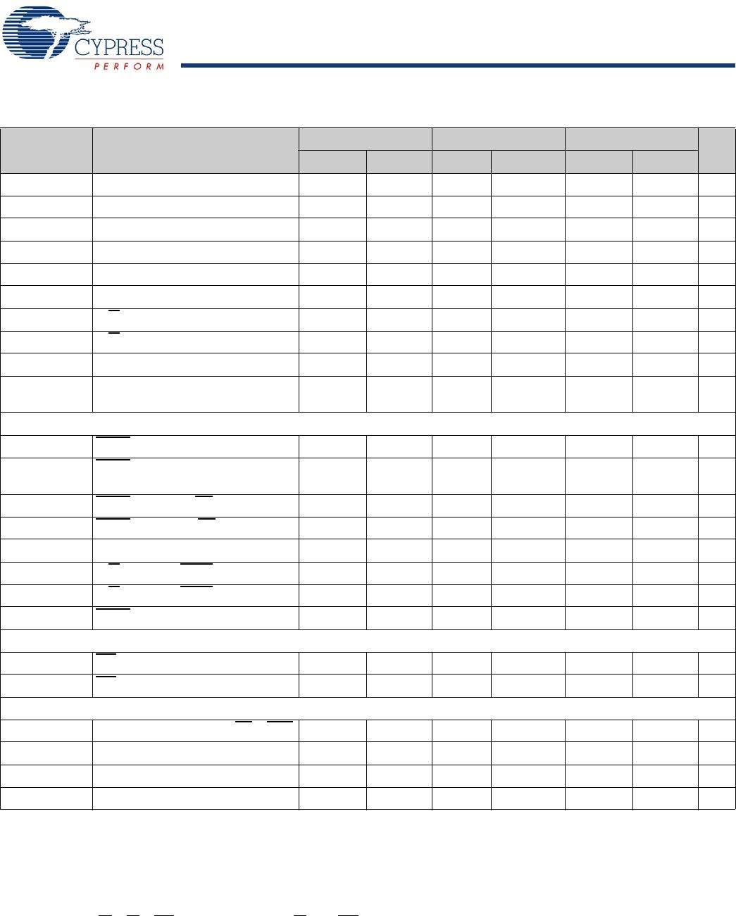
t
AW
Address setup to write end 12 – 20 – 35 – ns
t
HA
Address hold from write end 0 – 0 – 0 – ns
t
SA
[23]
Address setup to write start 0 – 0 – 0 – ns
t
PWE
Write pulse width 12 – 20 – 35 – ns
t
SD
Data setup to write end 10 – 15 – 20 – ns
t
HD
Data hold from write end 0 – 0 – 0 – ns
t
HZWE
[24, 25]
R/W LOW to high Z – 10 – 15 – 25 ns
t
LZWE
[24, 25]
R/W HIGH to low Z 3 – 3 – 3 – ns
t
WDD
[26]
Write pulse to data delay – 30 – 50 – 70 ns
t
DDD
[26]
Write data valid to read
data valid
–25–35 –45ns
Busy Timing
[27]
t
BLA
BUSY LOW from Address Match – 15 – 20 – 45 ns
t
BHA
BUSY HIGH from Address
Mismatch
–15–20 –40ns
t
BLC
BUSY LOW from CE LOW – 15 – 20 – 40 ns
t
BHC
BUSY HIGH from CE HIGH –15–20 –35ns
t
PS
Port Setup for Priority 5 – 5 – 5 – ns
t
WB
R/W HIGH after BUSY (Slave) 0 – 0 – 0 – ns
t
WH
R/W HIGH after BUSY HIGH (Slave) 13 – 20 – 40 – ns
t
BDD
[28]
BUSY HIGH to Data Valid – Note 28 Note 28 Note 28 ns
Interrupt Timing
[27]
t
INS
INT Set Time –15–20 –30ns
t
INR
INT Reset Time –15–20 –30ns
Semaphore Timing
t
SOP
SEM Flag Update Pulse (OE or SEM)10–12– 20–ns
t
SWRD
SEM Flag Write to Read Time 5 – 10 – 15 – ns
t
SPS
SEM Flag Contention Window 5 – 10 – 15 – ns
t
SAA
SEM Address Access Time – 15 25 – 55 ns
Switching Characteristics Over the Operating Range (continued)
[18]
Parameter Description
–15 –25 –55
Unit
Min Max Min Max Min Max
Notes
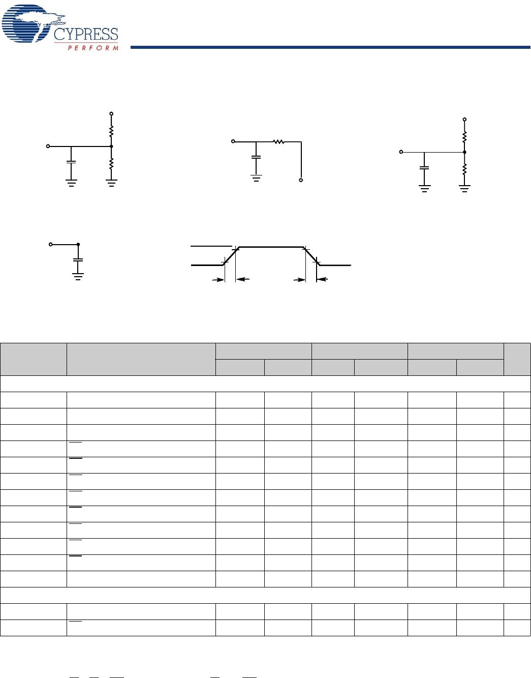
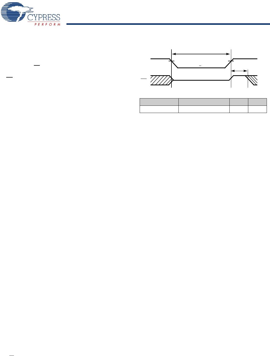
23. To access RAM, CE
=L, UB=L, SEM=H. To access semaphore, CE=H and SEM=L. Either condition must be valid for the entire t
SCE
time.
24. Test conditions used are Load 3.
25. This parameter is guaranteed but not tested.
26. For information on port-to-port delay through RAM cells from writing port to reading port, refer to Figure 11 on page 16.
27. Test conditions used are Load 2.
28. t
BDD
is a calculated parameter and is the greater of t
WDD
– t
PWE
(actual) or t
DDD
– t
SD
(actual).