74VHC_VHCT08_Q100 All information provided in this document is subject to legal disclaimers. © NXP B.V. 2013. All rights reserved.
Product data sheet Rev. 1 — 20 December 2013 6 of 15
NXP Semiconductors 74VHC08-Q100; 74VHCT08-Q100
Quad 2-input AND gate
10. Dynamic characteristics
For type 74VHCT08-Q100
V
IH
HIGH-level
input voltage
V
CC
= 4.5 V to 5.5 V 2.0 - - 2.0 - 2.0 - V
V
IL
LOW-level
input voltage
V
CC
= 4.5 V to 5.5 V - - 0.8 - 0.8 - 0.8 V
V
OH
HIGH-level
output voltage
V
I
= V
IH
or V
IL
; V
CC
= 4.5 V
I
O
= 50 A 4.4 4.5 - 4.4 - 4.4 - V
I
O
= 8.0 mA 3.94 - - 3.8 - 3.7 - V
V
OL
LOW-level
output voltage
V
I
= V
IH
or V
IL
; V
CC
= 4.5 V
I
O
= 50 A - 0 0.1 - 0.1 - 0.1 V
I
O
= 8.0 mA - - 0.36 - 0.44 - 0.55 V
I
I
input leakage
current
V
I
= 5.5 V or GND;
V
CC
= 0 V to 5.5 V
- - 0.1 - 1.0 - 2.0 A
I
CC
supply current V
I
=V
CC
or GND; I
O
= 0 A;
V
CC
=5.5V
--2.0- 20 - 40A
I
CC
additional
supply current
per input pin;
V
I
=V
CC
2.1 V; I
O
=0 A;
other pins at V
CC
or GND;
V
CC
= 4.5 V to 5.5 V
--1.35- 1.5 - 1.5mA
C
I
input
capacitance
- 3.0 10 - 10 - 10 pF
Table 6. Static characteristics …continued
Voltages are referenced to GND (ground = 0 V).
Symbol Parameter Conditions 25 C 40 C to +85 C 40 C to +125 C Unit
Min Typ Max Min Max Min Max
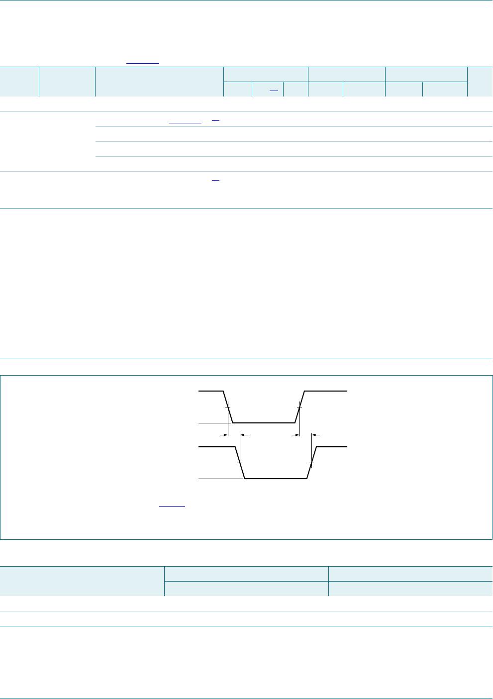
Table 7. Dynamic characteristics
GND = 0 V; For test circuit, see Figure 7
.
Symbol Parameter Conditions 25 C 40 C to +85 C 40 C to +125 C Unit
Min Typ
[1]
Max Min Max Min Max
For type 74VHC08-Q100
t
pd
propagation
delay
nA, nB to nY; see Figure 6
[2]
V
CC
= 3.0 V to 3.6 V
C
L
= 15 pF - 4.0 8.8 1.0 10.5 1.0 11.0 ns
C
L
= 50 pF - 5.6 12.3 1.0 14 1.0 15.5 ns
V
CC
= 4.5 V to 5.5 V
C
L
= 15 pF - 3.0 5.9 1.0 7.0 1.0 7.5 ns
C
L
= 50 pF 4.2 7.9 1.0 9.0 1.0 10.0 ns
C
PD
power
dissipation
capacitance
C
L
=50pF; f
i
= 1 MHz;
V
I
=GNDtoV
CC
[3]
- 10.0 - - - - - pF