VS-30BQ040-M3/9AT

VS-30BQ040-M3
www.vishay.com
Vishay Semiconductors
Revision: 18-Nov-15
4
Document Number: 93332
For technical questions within your region: DiodesAmericas@vishay.com
, DiodesAsia@vishay.com, DiodesEurope@vishay.com
THIS DOCUMENT IS SUBJECT TO CHANGE WITHOUT NOTICE. THE PRODUCTS DESCRIBED HEREIN AND THIS DOCUMENT
ARE SUBJECT TO SPECIFIC DISCLAIMERS, SET FORTH AT www.vishay.com/doc?91000
Fig. 5 - Maximum Average Forward Current vs.
Allowable Lead Temperature
Fig. 6 - Maximum Average Forward Dissipation vs.
Average Forward Current
Fig. 7 - Maximum Peak Surge Forward Current vs. Pulse Duration
Note
(1)
Formula used: T
C
= T
J
- (Pd + Pd
REV
) x R
thJC
;
Pd = Forward power loss = I
F(AV)
x V
FM
at (I
F(AV)
/D) (see fig. 6);
Pd
REV
= Inverse power loss = V
R1
x I
R
(1 - D); I
R
at V
R1
= 80 % rated V
R
60
80
100
120
140
160
Allowable Lead Temperature (°C)
I
F(AV)
- Average Forward Current (A)
0.5 2.5 4.53.51.51.0 3.0 4.02.00
Square wave (D = 0.50)
80 % rated V
R
applied
See note (1)
D = 0.20
D = 0.25
D = 0.33
D = 0.50
D = 0.75
DC
0
1.0
1.5
0.5
2.5
2.0
Average Power Loss (W)
I
F(AV)
- Average Forward Current (A)
0.5 1.5 3.0
4.5
3.5 4.02.01.00
2.5
DC
RMS limit
D = 0.75
D = 0.50
D = 0.33
D = 0.25
D = 0.20
1
10
1000
100
10 000
I
FSM
- Non-Repetitive Surge Current (A)
t
p
- Square Pulse Duration (µs)
10 000100010010
At any rated load condition
and with rated V
RRM
applied
following surge
VS-30BQ040-M3
www.vishay.com
Vishay Semiconductors
Revision: 18-Nov-15
5
Document Number: 93332
For technical questions within your region: DiodesAmericas@vishay.com
, DiodesAsia@vishay.com, DiodesEurope@vishay.com
THIS DOCUMENT IS SUBJECT TO CHANGE WITHOUT NOTICE. THE PRODUCTS DESCRIBED HEREIN AND THIS DOCUMENT
ARE SUBJECT TO SPECIFIC DISCLAIMERS, SET FORTH AT www.vishay.com/doc?91000
ORDERING INFORMATION TABLE
ORDERING INFORMATION (Example)
PREFERRED P/N PREFERRED PACKAGE CODE MINIMUM ORDER QUANTITY PACKAGING DESCRIPTION
VS-30BQ040-M3/9AT 9AT 3500 13" diameter plastic tape and reel
LINKS TO RELATED DOCUMENTS
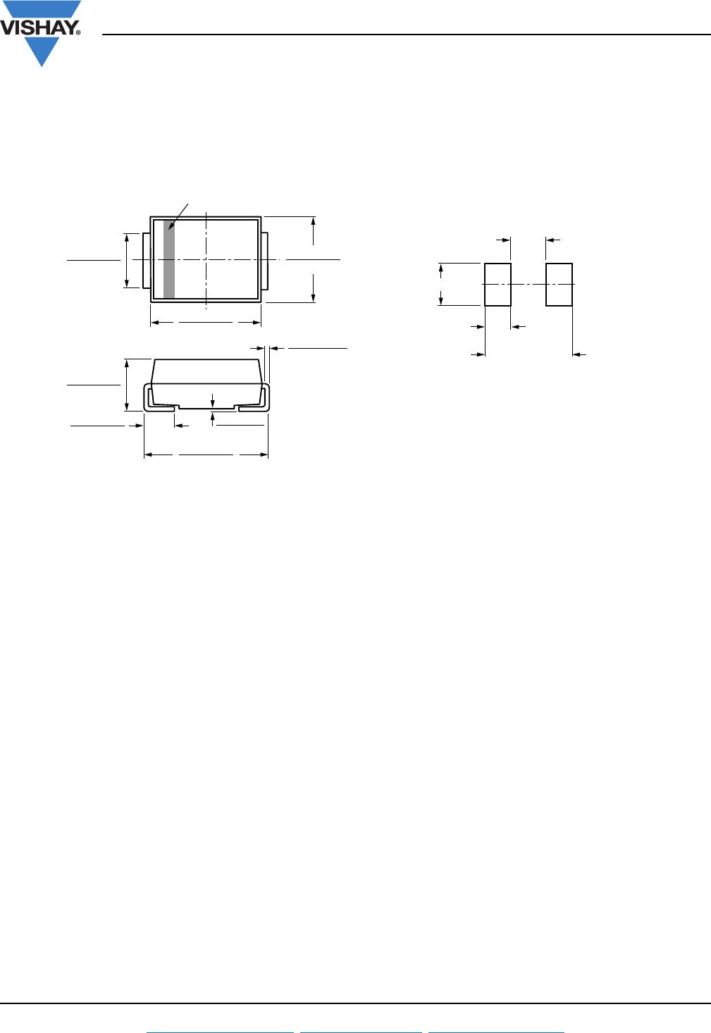
Dimensions www.vishay.com/doc?95402
Part marking information www.vishay.com/doc?95403
Packaging information www.vishay.com/doc?95404
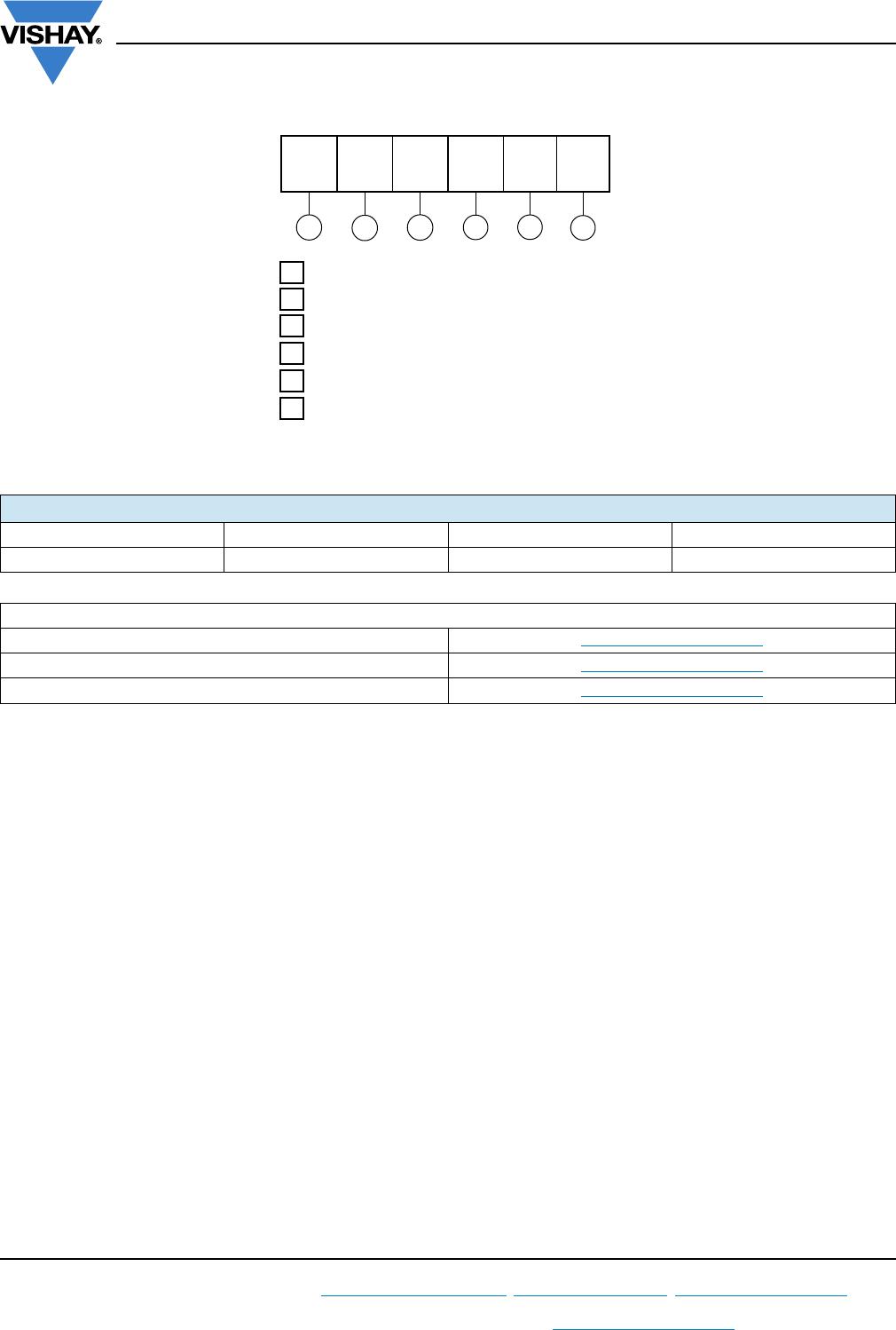
2 - Current rating
3 - B = SMC
4
- Q = Schottky “Q” series
5 - Voltage rating (040 = 40 V)
1 - Vishay Semiconductors product
Device code
51 32 4 6
VS- 30 B Q 040 -M3
- Environmental digit:
-M3 = halogen-free, RoHS-compliant, and terminations lead (Pb)-free
6
Document Number: 95402 For technical questions within your region, please contact one of the following: www.vishay.com
Revision: 09-Jul-10 DiodesAmericas@vishay.com
, DiodesAsia@vishay.com, DiodesEurope@vishay.com 1
SMC
Outline Dimensions
Vishay Semiconductors
DIMENSIONS in inches (millimeters)
Cathode band
DO-214AB (SMC)
0.126 (3.20)
0.114 (2.90)
0.246 (6.22)
0.220 (5.59)
0.280 (7.11)
0.260 (6.60)
0.012 (0.305)
0.006 (0.152)
0.008 (0.2)
0 (0)
0.320 (8.13)
0.305 (7.75)
0.060 (1.52)
0.030 (0.76)
0.103 (2.62)
0.079 (2.06)
Mounting Pad Layout
0.126 (3.20) MIN.
0.060 (1.52) MIN.
0.185 (4.69) MAX.
0.320 (8.13) REF.

VS-30BQ040-M3/9AT

Mfr. #:
Manufacturer:
Vishay Semiconductors
Description:
Schottky Diodes & Rectifiers 3A 40V Single Die Schottky Rectifier
Lifecycle:
New from this manufacturer.
Delivery:
DHL FedEx Ups TNT EMS
Payment:
T/T Paypal Visa MoneyGram Western Union

Products related to this Datasheet