11
FN8165.3
August 29, 2006
ABSOLUTE MAXIMUM RATINGS
Temperature under bias ........................ -65 to +135°C
Storage temperature ............................. -65 to +150°C
Voltage on SCK, SCL or any address input
with respect to V
SS
................................. -1V to +7V
Voltage on V+ (referenced to V
SS
)........................ 10V
Voltage on V- (referenced to V
SS
)........................-10V
(V+) - (V-) .............................................................. 12V
Any V
H
/R
H
..............................................................V+
Any V
L
/R
L
.................................................................V-
Lead temperature (soldering, 10s) .................. +300°C
I
W
(10s) ............................................................±15mA
COMMENT
Stresses above those listed under “Absolute Maximum
Ratings” may cause permanent damage to the device.
This is a stress rating only; functional operation of the
device (at these or any other conditions above those
listed in the operational sections of this specification) is
not implied. Exposure to absolute maximum rating
conditions for extended periods may affect device
reliability.
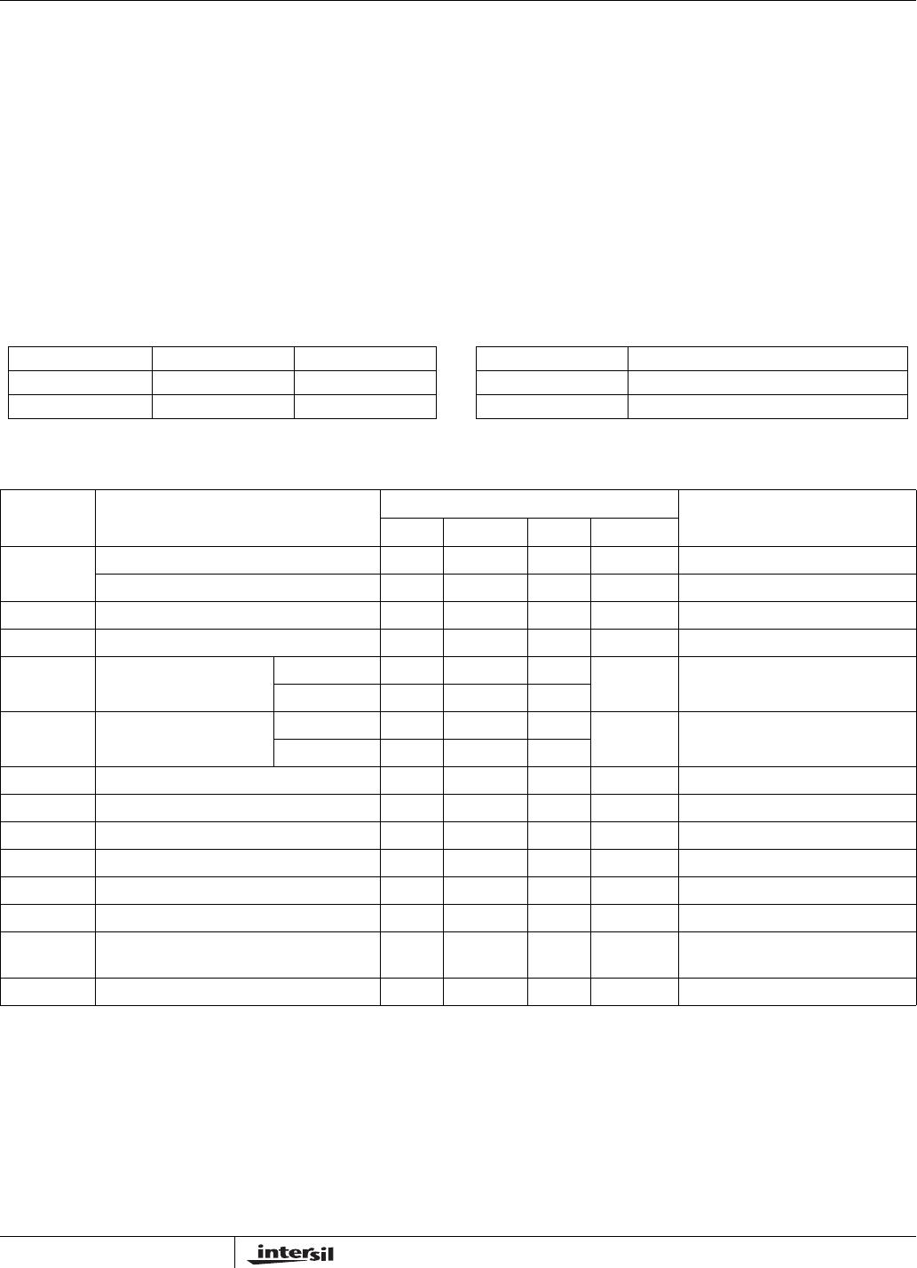
POTENTIOMETER CHARACTERISTICS
(Over recommended operating conditions unless otherwise stated.)
Notes: (1) Absolute linearity is utilized to determine actual wiper voltage versus expected voltage as determined by wiper position when used as a
potentiometer.
(2) Relative linearity is utilized to determine the actual change in voltage between two successive tap positions when used as a potentiom-
eter. It is a measure of the error in step size.
(3) MI = RTOT/255 or (V
H
/R
H
- V
L
/R
L
)/255, single pot
(4) Individual array resolutions.
Symbol Parameter
Limits
Test ConditionsMin. Typ. Max. Unit
End to end resistance tolerance ±20 %
Power rating 50 mW +25°C, each pot
I
W
Wiper current ±7.5 mA
R
W
Wiper resistance 150 250 Ω Wiper current = ± 1mA
Vv+ Voltage on V+ pin X9250 +4.5 +5.5 V
X9250-2.7 +2.7 +5.5
Vv- Voltage on V- pin X9250 -5.5 -4.5 V
X9250-2.7 -5.5 -2.7
V
TERM
Voltage on any V
H
/R
H
or V
L
/R
L
pin V- V+ V
Noise -120 dBV Ref: 1kHz
Resolution
(4)
0.6 %
Absolute linearity
(1)
±1 MI
(3)
V
w(n)(actual)
- V
w(n)(expected)
Relative linearity
(2)
±0.6 MI
(3)
V
w(n + 1 -
[V
w(n) + MI
]
Temperature coefficient of R
TOTAL
±300 ppm/°C
Ratiometric Temperature
Coefficient
±20 ppm/°C
C
H
/C
L
/C
W
Potentiometer Capacitances 10/10/25 pF See Circuit #3
RECOMMENDED OPERATING CONDITIONS
Temp Min. Max.
Commercial 0°C+70°C
Industrial -40°C+85°C
Device Supply Voltage (V
CC
) Limits
(4)
X9250 5V ±10%
X9250-2.7 2.7V to 5.5V
X9250