AOT10N60/AOB10N60/AOTF10N60
TYPICAL ELECTRICAL AND THERMAL CHARACTERISTICS
0.001
0.01
0.1
1
10
0.00001 0.0001 0.001 0.01 0.1 1 10 100
Pulse Width (s)
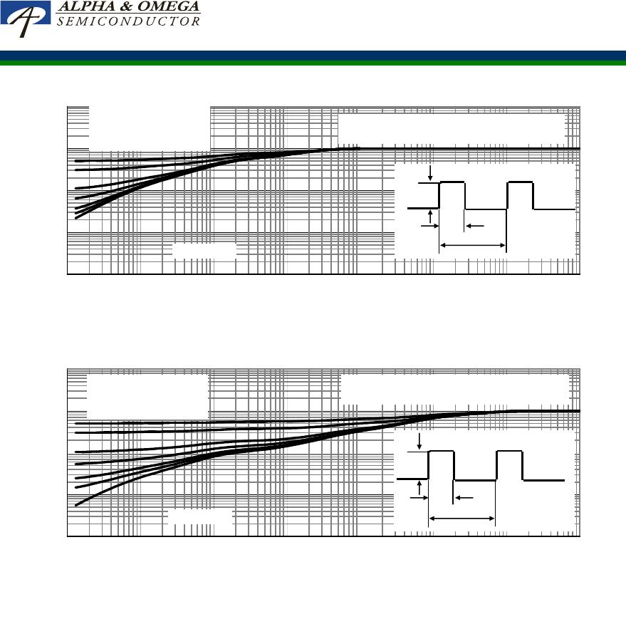
Figure 12: Normalized Maximum Transient Thermal Impedance for AOT10N60/AOB10N60 (Note F)
Z
θ
θ
θ
θ
JC
Normalized Transient
Thermal Resistance
D=T
on
/T
T
J,PK
=T
C
+P
DM
.Z
θJC
.R
θJC
R
θJC
=0.5°C/W
In descending order
D=0.5, 0.3, 0.1, 0.05, 0.02, 0.01, single pulse
T
on
T
P
Single Pulse
0.001
0.01
0.1
1
10
0.00001 0.0001 0.001 0.01 0.1 1 10 100
Pulse Width (s)
Figure 13: Normalized Maximum Transient Thermal Impedance for AOTF10N60 (Note F)
Z
θ
θ
θ
θ
JC
Normalized Transient
Thermal Resistance
D=T
on
/T
T
J,PK
=T
C
+P
DM
.Z
θJC
.R
θJC
R
θJC
=2.5°C/W
In descending order
D=0.5, 0.3, 0.1, 0.05, 0.02, 0.01, single pulse
Single Pulse
T
on
T
P
D
Rev7: Jul 2011 www.aosmd.com Page 5 of 6

