40V, Ultra-Low Quiescent-Current
Linear Regulators in 6-Pin TDFN/8-Pin SO
Maxim Integrated 7
MAX15006/MAX15007
OUTPUT VOLTAGE NOISE
vs. OUTPUT CAPACITANCE
MAX15006 toc26
C
OUT
(μF)
e
n
(μV
RMS
)
1412810462
15
30
45
60
75
90
105
120
135
150
0
0221816 20
MAX15006A/MAX15007A
I
OUT
= 25mA
CLAMPED LOAD DUMP
(I
OUT
= 0)
MAX15006 toc27
100ms/div
40V
V
IN
13.5V
V
OUT
AC-COUPLED
20mV/div
Typical Operating Characteristics (continued)
(V
IN
= 14V, C
IN
= 0.1μF, C
OUT
= 2.2μF, V
EN
= V
IN
, T
A
= +25°C, unless otherwise noted.)
Pin Description
PIN
MAX15006A/B MAX15006C MAX15007A/B MAX15007C
TDFN SO TDFN SO TDFN SO TDFN SO
NAME FUNCTION
1, 2 1 1, 2 1 1, 2 1 1, 2 1 IN
Regulator Supply Input. Supply voltage ranges
from 4V to 40V. Bypass with a 0.1μF capacitor to
GND.
3
2, 3,
4, 6, 7
3
2, 3, 4,
6
2, 4, 6,
7
2, 4, 6 N.C. No Connection. Not internally connected.
45454545GNDGround
5, 6 8 6 8 5, 6 8 6 8 OUT
Regulator Output. Bypass OUT to GND with a
low-ESR capacitor with a minimum 2.2μF.
5757FB
Feedback Regulation Set-Point. Connect an
external resistive divider network from OUT to FB
to GND to adjust the output voltage from 1.8V to
10V.
———— 3 3 3 3 EN
Active-High Enable Input. Force EN high (or
connect to V
IN
) to turn the regulator on. Pull EN
low (or leave unconnected) to place the device
in a low-power shutdown mode. EN is internally
pulled down to GND through a 0.5μA sink
current.
————————EP
Exposed Pad. Internally connected to GND.
Connect EP to the ground plane for enhanced
thermal performance. Do not use EP as a
ground connection.
40V, Ultra-Low Quiescent-Current
Linear Regulators in 6-Pin TDFN/8-Pin SO
8 Maxim Integrated
MAX15006/MAX15007
MAX15006
FET DRIVER
WITH
CURRENT LIMIT
THERMAL
SENSOR
1.242V
REF
ERROR
AMPLIFIER
+
-
OUT
FB
(FOR MAX15006C ONLY)
(FOR MAX15006A/B ONLY)
IN
GND
Figure 1. MAX15006 Simplified Functional Diagram
Functional Diagrams
MAX15007
FET DRIVER
WITH
CURRENT LIMIT
THERMAL
SENSOR
CONTROL
LOGIC
1.242V
REF
ERROR
AMPLIFIER
+
-
OUT
IN
EN
GND
FB
(FOR MAX15007C ONLY)
(FOR MAX150076A/B ONLY)
Figure 2. MAX15007 Simplified Functional Diagram
40V, Ultra-Low Quiescent-Current
Linear Regulators in 6-Pin TDFN/8-Pin SO
Maxim Integrated 9
MAX15006/MAX15007
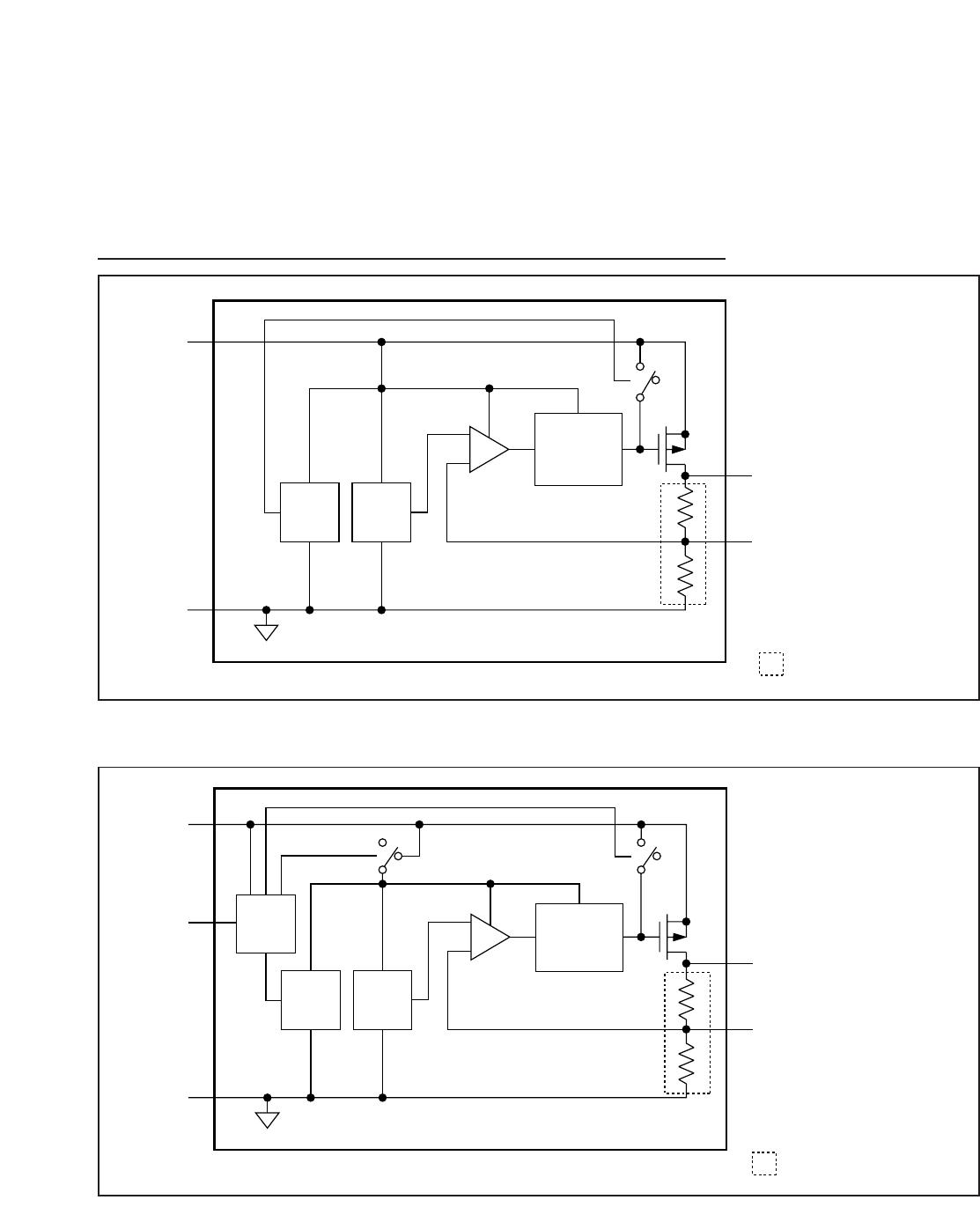
Detailed Description
The MAX15006/MAX15007 high-voltage linear regulators
operate over a 4V to 40V input voltage range. These
devices guarantee 50mA load drive, and offer preset
output voltages of +3.3V (MAX15006A/MAX15007A) or
+5V (MAX15006B/MAX15007B) or an adjustable voltage
output from 1.8V to 10V (MAX15006C/MAX15007C).
Thermal shutdown and short-circuit protection prevent
damage during overtemperature and overcurrent condi-
tions. The MAX15007 includes an enable input (EN)
allowing the regulators to be turned on/off using a logic-
level voltage. Driving EN high turns on the device while
driving EN low places the device in a low-power shut-
down mode. In shutdown, the supply current is reduced
to 3μA (typ). The MAX15006/MAX15007 operate over the
-40°C to +125°C automotive temperature range. All
devices are available in thermally enhanced 6-pin TDFN
and 8-pin SO packages capable of dissipating 1.904W
and 1.860W at T
A
= +70°C, respectively.
Regulator
The regulator accepts an input voltage from 4V to 40V.
The MAX15006A/MAX15007A have a fixed 3.3V output
voltage while the MAX15006B/MAX15007B offer a fixed
5V output voltage. The MAX15006C/MAX15007C fea-
ture an adjustable voltage output by connecting an
external resistive divider from OUT to FB and to GND
(see the
Output Voltage Setting
section).
EN Input (MAX15007 Only)
EN is an active-high, logic-level enable input that turns
the device on or off. Drive EN high to turn the device
on. An internal 0.5μA pulldown current keeps the
MAX15007 in shutdown mode when driven by a three-
state driver in high-impedance mode, or an open-drain
driver. While in shutdown, the device consumes only
3μA (typ). EN withstands voltages up to 40V, allowing it
to be driven by high input level voltages or connected
to IN for always-on operation.
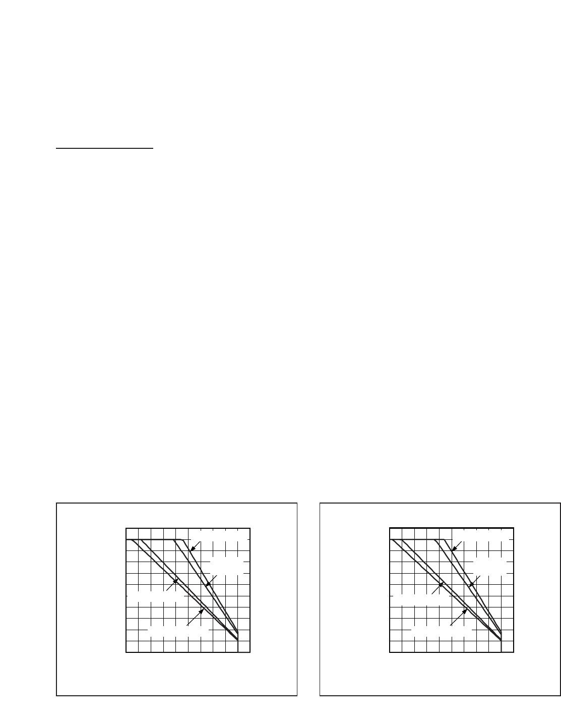
Thermal Protection
When the junction temperature exceeds +165°C, an
internal thermal sensor turns the pass transistor off, and
allows the device to cool. The thermal sensor turns the
pass transistor on again after the junction temperature
cools by 20°C. This results in a cycled output during
continuous thermal-overload conditions. Thermal pro-
tection protects the MAX15006/MAX15007 in the event
of fault conditions. Operation at T
J
= +150°C without
going into thermal shutdown is not guaranteed. Use
Figures 3a and 3b to determine the minimum guaran-
teed output current.
Output Short-Circuit Current Limit
The MAX15006/MAX15007 feature a 175mA current
limit. The output can be shorted to GND for an indefinite
period of time without damage to the device. During a
short circuit, the power dissipated across the pass tran-
sistor can quickly heat the device. When the die tem-
perature reaches +165°C, the MAX15006/
MAX15007 shut down and automatically restart after
the die temperature cools by 20°C.
MAX15006 fig03a
AMBIENT TEMPERATURE (°C)
OUTPUT CURRENT (mA)
125120110 11590 95 100 10585
5
10
15
20
25
30
35
40
45
50
55
0
80 130
V
IN
= 26V, V
OUT
= 5V
V
IN
= 18V, V
OUT
= 5V
V
IN
= 18V,
V
OUT
= 3.3V
V
IN
= 26V, V
OUT
= 3.3V
Figure 3a. Minimum Output Current vs. Ambient Temperature
(6-Pin TDFN-EP)
MAX15006 fig03b
AMBIENT TEMPERATURE (°C)
OUTPUT CURRENT (mA)
125120110 11590 95 100 10585
5
10
15
20
25
30
35
40
45
50
55
0
80 130
V
IN
= 26V, V
OUT
= 5V
V
IN
= 18V, V
OUT
= 5V
V
IN
= 18V,
V
OUT
= 3.3V
V
IN
= 26V, V
OUT
= 3.3V
Figure 3b. Minimum Output Current vs. Ambient Temperature
(8-Pin SO-EP)

MAX15007AATT+

Mfr. #:
Manufacturer:
Maxim Integrated
Description:
Linear Voltage Regulators 40V, Ultra-Low Quiescent-Current Linear Regulators in 6-Pin TDFN/8-Pin SO
Lifecycle:
New from this manufacturer.
Delivery:
DHL FedEx Ups TNT EMS
Payment:
T/T Paypal Visa MoneyGram Western Union