NE696M01-T1

NE696M01
NEC's NPN SILICON HIGH
FREQUENCY TRANSISTOR
HIGH fT:
14 GHz TYP at 3 V, 10 mA
LOW NOISE FIGURE:
NF = 1.6 dB TYP at 2 GHz
HIGH GAIN:
|S
21E|
2
= 14 dB TYP at 2 GHz
6 PIN SMALL MINI MOLD PACKAGE
EXCELLENT LOW VOLTAGE, LOW CURRENT
PERFORMANCE
FEATURES OUTLINE DIMENSIONS (Units in mm)
PACKAGE OUTLINE M01
DESCRIPTION
NEC's NE696M01 is an NPN high frequency silicon epitaxial
transistor (NE685) encapsulated in an ultra small 6 pin SOT-
363 package. Its four emitter pins decrease emitter inductance
resulting in 3 dB more gain compared to conventional SOT-23
and SOT-143 devices. The NE696M01 is ideal for LNA and
pre-driver applications up to 2.4 GHz where low cost, high gain,
low voltage and low current are prime considerations.
California Eastern Laboratories
3. For Tape and Reel version use part number NE696M01-T1, 3K per reel.
PART NUMBER NE696M01
PACKAGE OUTLINE M01
SYMBOLS PARAMETERS AND CONDITIONS UNITS MIN TYP MAX
ICBO Collector Cutoff Current at VCB = 5 V, IE = 0 µA 0.1
IEBO Emitter Cutoff Current at VEB = 1 V, IC = 0 µA 0.1
hFE
1
Forward Current Gain at VCE = 3 V, IC = 10 mA 80 120 160
fT Gain Bandwidth at VCE = 3 V, IC = 10 mA, f = 2 GHz GHz 14
Cre
2
Feedback Capacitance at VCB = 3 V, IE = 0, f = 1 MHz pF 0.15
|S21E|
2
Insertion Power Gain at VCE = 3 V, IC = 10 mA, f = 2 GHz dB 14
NF Noise Figure at VCE = 3 V, IC = 3 mA, f = 2 GHz dB 1.6
ELECTRICAL CHARACTERISTICS (TA = 25°C)
Notes:
1. Pulsed measurement, pulse width 350 µs, duty cycle 2 %.
2.The emitter terminal should be connected to the ground terminal of the 3 terminal capacitance bridge.
2.1 ± 0.1
1.25 ± 0.1
0 ~ 0.1
0.15
0.9 ± 0.1
0.7
2.0 ± 0.2
0.65
1.3
1
2
3
4
5
6
0.2 (All Leads)
+0.10
- 0.05
T95
TOP VIEW
SIDE VIEW
Note:
Pin 3 is identified with a circle on the bottom of the package.
PIN OUT
1. Emitter
2. Emitter
3. Base
4. Emitter
5. Emitter
6. Collector
ABSOLUTE MAXIMUM RATINGS
1
(TA = 25°C)
SYMBOLS PARAMETERS UNITS RATINGS
V
CBO Collector to Base Voltage V 9
V
CEO Collector to Emitter Voltage V 6
V
EBO Emitter to Base Voltage V 2
I
C Collector Current mA 30
P
T Total Power Dissipation mW 150
TJ Junction Temperature °C 150
TSTG Storage Temperature °C -65 to +150
Notes:
1. Operation in excess of any one of these parameters may result
in permanent damage.
NE696M01
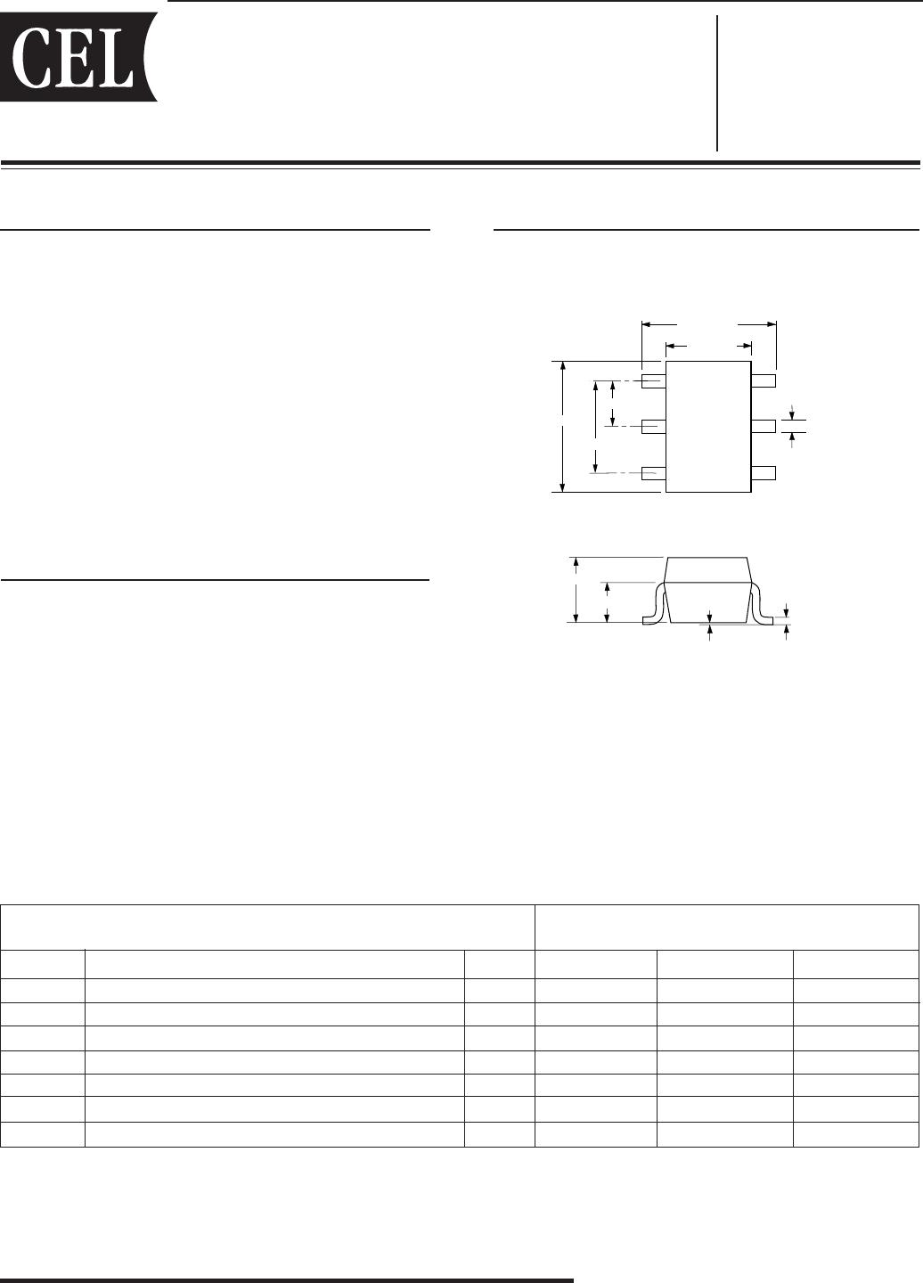
PART NUMBER QUANTITY PACKAGING
NE696M01-T1-A 3000 Tape & Reel
VCE = 1 V, IC = 3 mA
1.0 1.4 18.5 0.53 79 0.27
1.4 1.46 16.4 0.47 95 0.13
1.7 1.55 15.2 0.43 111 0.19
2.0 1.8 14.5 0.39 132 0.16
3.0 2.3 11.0 0.3 177 0.10
V
CE = 2 V, IC = 1 mA
FREQ. NFOPT GA
ΓΓ
ΓΓ
Γ
OPT
(GHz) (dB) (dB) MAG ANG Rn/50
NE696M01
TYPICAL NOISE PARAMETERS (TA = 25˚C)
0.5 .94 16.8 0.72 41 0.52
0.8 1.1 14.8 0.66 65 0.44
1.0 1.25 13.8 0.63 79 0.39
1.5 1.55 11.4 0.56 104 0.31
2.0 1.94 9.6 0.5 138 0.17
3.0 2.65 7.0 0.46 -173 0.07
0.5 1.2 23.0 0.49 37 0.38
0.8 1.32 20.3 0.44 62 0.27
1.0 1.47 18.8 0.42 76 0.30
1.5 1.63 15.8 0.39 98 0.23
2.0 1.82 13.0 0.33 126 0.18
3.0 2.17 9.8 0.25 173 0.10
VCE = 2 V, IC = 5 mA
VCE = 3 V, IC = 5 mA
0.5 1.25 24.2 0.5 37 0.39
0.8 1.35 20.7 0.45 62 0.26
1.0 1.41 18.8 0.44 78 0.29
1.5 1.58 15.2 0.41 97 0.24
2.0 1.81 13.7 0.34 126 0.20
3.0 2.29 12.0 0.29 164 0.09
ORDERING INFORMATION
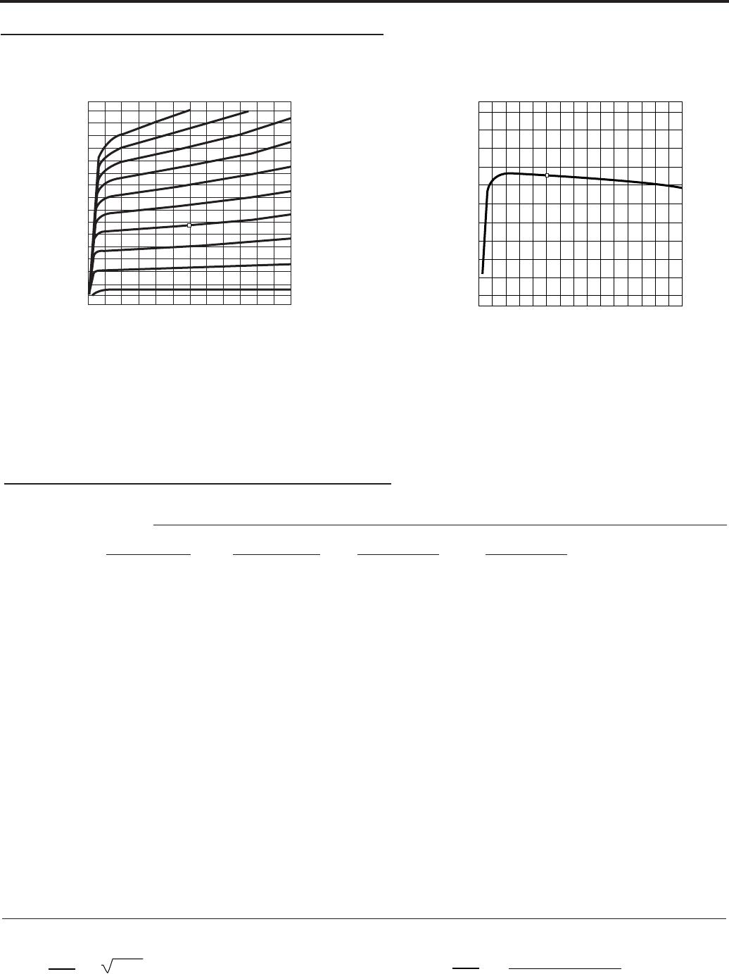
TYPICAL PERFORMANCE CURVES (TA = 25˚C)
0
10
20
30
40
50
0.5 1.0
V
CE
= 2 V
TOTAL POWER DISSIPATION vs.
AMBIENT TEMPERATURE
COLLECTOR CURRENT vs.
BASE TO EMITTER VOLTAGE
Total Power Dissipation, P
T
(mW)
Ambient Temperature, TA (˚C)
Collector Current, I
C
(mA)
Base to Emitter Voltage, VBE (V)
25
20
15
10
5
0
1.0 2.0 3.0
200 µA
180 µA
160 µA
140 µA
120 µA
100 µA
80 µA
60 µA
40 µA
I
B
= 20 µA
500
200
100
50
20
10
1 2 5 10 20 50 100
V
CE
= 2 V
V
CE
= 1 V
COLLECTOR CURRENT vs.
COLLECTOR TO EMITTER VOLTAGE
DC CURRENT GAIN vs.
COLLECTOR CURRENT
Collector Current, IC (mA)
DC Current Gain, hFE
Collector Current, I
C
(mA)
Collector to Emitter Voltage, VCE (V)
200
100
0
0 50 100 150
NE696M01
TYPICAL PERFORMANCE CURVES (TA = 25 °C)
Collector to Emitter Voltage, VCE (V)
COLLECTOR CURRENT vs.
COLLECTOR TO EMITTER VOLTAGE
DC CURRENT GAIN vs.
COLLECTOR CURRENT
Collector Current, I
C
(mA)
DC Current Gain, h
FE
(mA)
Collector Current, IC (mA)
30.0m
2.00m
/div
0.00
0.00 VCE (V) 500m /div 6.00
IC
150.0
10.0
/div
50.0
0.00 IC (A) 2.00m /div 30.0m
HFE
NE696M01
VCE = 1 V, IC = 5 mA
FREQUENCY S11 S21 S12 S22 K MAG
1
(GHz) MAG ANG MAG ANG MAG ANG MAG ANG (dB)
0.40 0.728 -52.30 10.962 136.50 0.040 56.00 0.832 -32.90 0.303 24.378
0.50 0.684 -64.20 10.349 128.40 0.046 51.30 0.779 -39.10 0.338 23.521
0.60 0.639 -73.80 9.557 121.20 0.052 46.70 0.732 -44.00 0.398 22.643
0.70 0.594 -83.40 8.885 114.50 0.056 42.10 0.687 -48.50 0.463 22.005
0.80 0.556 -92.50 8.236 108.30 0.059 38.80 0.647 -52.30 0.522 21.449
0.90 0.522 -100.70 7.644 102.80 0.062 35.70 0.615 -55.70 0.579 20.909
1.00 0.492 -108.50 7.116 97.80 0.063 33.80 0.587 -58.60 0.640 20.529
1.20 0.442 -123.40 6.242 88.70 0.067 29.60 0.542 -64.10 0.748 19.692
1.40 0.406 -137.30 5.522 80.40 0.069 26.80 0.509 -69.10 0.860 19.032
1.60 0.380 -150.60 4.931 73.00 0.070 24.40 0.485 -73.40 0.976 18.478
1.80 0.362 -164.30 4.452 65.90 0.072 22.70 0.469 -77.90 1.069 16.304
2.00 0.353 -176.70 4.047 59.30 0.074 21.90 0.459 -81.80 1.151 15.018
2.25 0.351 167.30 3.606 51.40 0.075 20.20 0.451 -86.70 1.270 13.695
2.50 0.360 152.60 3.248 43.80 0.077 20.20 0.449 -91.40 1.353 12.702
2.75 0.377 138.80 2.942 36.40 0.079 19.30 0.453 -96.10 1.417 11.872
3.00 0.397 127.30 2.676 29.70 0.081 18.50 0.458 -100.50 1.475 11.110
3.50 0.451 107.70 2.251 16.40 0.085 18.50 0.477 -108.90 1.530 9.936
4.00 0.498 93.20 1.930 4.10 0.092 17.50 0.496 -118.00 1.515 8.980
4.50 0.538 82.30 1.690 -7.90 0.101 16.20 0.513 -128.80 1.460 8.216
5.00 0.567 74.10 1.509 -19.70 0.113 13.60 0.532 -142.40 1.371 7.622
5.50 0.587 67.30 1.361 -31.50 0.127 9.40 0.555 -158.60 1.283 7.107
6.00 0.608 61.10 1.229 -43.20 0.141 4.00 0.593 -175.70 1.175 6.870
6.50 0.630 55.20 1.091 -54.40 0.155 -1.40 0.637 168.60 1.077 6.778
7.00 0.657 49.10 0.949 -63.80 0.164 -6.40 0.678 157.90 1.009 7.057
7.50 0.690 42.90 0.818 -70.40 0.171 -9.20 0.719 154.80 0.911 6.798
TYPICAL SCATTERING PARAMETERS (TA = 25°C)
MAG = Maximum Available Gain
MSG = Maximum Stable Gain
Note:
1. Gain Calculation:
MAG =
|S
21
|
|S
12
|
K - 1
).
2
(
K ±
= S
11
S
22
- S
21
S
12
When K 1, MAG is undefined and MSG values are used.
MSG =
|S
21
|
|S
12
|
, K =
1 + | | - |S
11
| - |S
22
|
2
2
2
2 |S
12
S
21
|
,

NE696M01-T1

Mfr. #:
Manufacturer:
CEL
Description:
RF Bipolar Transistors DISC BY CEL 1/02 M01 NPN HIGH FREQ
Lifecycle:
New from this manufacturer.
Delivery:
DHL FedEx Ups TNT EMS
Payment:
T/T Paypal Visa MoneyGram Western Union

Products related to this Datasheet