S3BHE3/9AT

S3A, S3B, S3D, S3G, S3J, S3K, S3M
www.vishay.com
Vishay General Semiconductor
Revision: 19-Feb-16
1
Document Number: 88713
For technical questions within your region: DiodesAmericas@vishay.com
, DiodesAsia@vishay.com, DiodesEurope@vishay.com
THIS DOCUMENT IS SUBJECT TO CHANGE WITHOUT NOTICE. THE PRODUCTS DESCRIBED HEREIN AND THIS DOCUMENT
ARE SUBJECT TO SPECIFIC DISCLAIMERS, SET FORTH AT www.vishay.com/doc?91000
Surface Mount Glass Passivated Rectifier
FEATURES
Low profile package
Ideal for automated placement
Glass passivated pellet chip junction
Low forward voltage drop
Low leakage current
High forward surge capability
Meets MSL level 1, per J-STD-020, LF maximum peak of
260 °C
AEC-Q101 qualified
Material categorization: for definitions of compliance
please see www.vishay.com/doc?99912
TYPICAL APPLICATIONS
For use in general purpose rectification of power supplies,
inverters, converters, and freewheeling diodes for
consumer, automotive, and telecommunication.
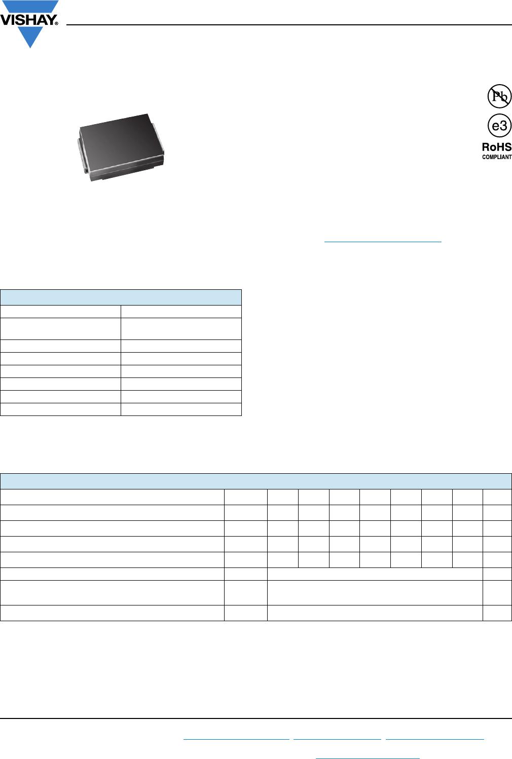
MECHANICAL DATA
Case: DO-214AB (SMC)
Molding compound meets UL 94 V-0 flammability rating
Base P/N-E3 - RoHS-compliant, commercial grade
Base P/NHE3_X - RoHS-compliant and AEC-Q101 qualified
(“_X” denotes revision code e.g. A, B,.....)
Terminals: Matte tin plated leads, solderable per
J-STD-002 and JESD 22-B102
E3 suffix meets JESD 201 class 2 whisker test, HE3 suffix
meets JESD 201 class 2 whisker test
Polarity: Color band denotes cathode end
PRIMARY CHARACTERISTICS
I
F(AV)
3.0 A
V
RRM
50 V, 100 V, 200 V, 400 V, 600 V,
800 V, 1000 V
I
FSM
100 A
I
R
10 μA
V
F
1.15 V
T
J
max. 150 °C
Package DO-214AB (SMC)
Diode variations Single die
DO-214AB (SMC)
MAXIMUM RATINGS (T
A
= 25 °C unless otherwise noted)
PARAMETER SYMBOL S3A S3B S3D S3G S3J S3K S3M UNIT
Device marking code SA SB SD SG SJ SK SM
Maximum recurrent peak reverse voltage V
RRM
50 100 200 400 600 800 1000 V
Maximum RMS voltage V
RMS
35 70 140 280 420 560 700 V
Maximum DC blocking voltage V
DC
50 100 200 400 600 800 1000 V
Maximum average forward rectified current at T
L
= 103 °C I
F(AV)
3.0 A
Peak forward surge current 8.3 ms single half sine-wave
superimposed on rated load
I
FSM
100 A
Operating junction and storage temperature range T
J
, T
STG
-55 to +150 °C
S3A, S3B, S3D, S3G, S3J, S3K, S3M
www.vishay.com
Vishay General Semiconductor
Revision: 19-Feb-16
2
Document Number: 88713
For technical questions within your region: DiodesAmericas@vishay.com
, DiodesAsia@vishay.com, DiodesEurope@vishay.com
THIS DOCUMENT IS SUBJECT TO CHANGE WITHOUT NOTICE. THE PRODUCTS DESCRIBED HEREIN AND THIS DOCUMENT
ARE SUBJECT TO SPECIFIC DISCLAIMERS, SET FORTH AT www.vishay.com/doc?91000
Note
(1)
Thermal resistance from junction to ambient and from junction to lead mounted on PCB with 0.3" x 0.3" (8.0 mm x 8.0 mm) copper pad area
Note
(1)
AEC-Q101 qualified
RATINGS AND CHARACTERISTICS CURVES (T
A
= 25 °C unless otherwise noted)
Fig. 1 - Forward Current Derating Curve Fig. 2 - Maximum Non-Repetitive Peak Forward Surge Current
ELECTRICAL CHARACTERISTICS (T
A
= 25 °C unless otherwise noted)
PARAMETER TEST CONDITIONS SYMBOL S3A S3B S3D S3G S3J S3K S3M UNIT
Maximum instantaneous forward voltage 2.5 A V
F
1.15 V
Maximum DC reverse current at rated
DC blocking voltage
T
A
= 25 °C
I
R
10
μA
T
A
= 125 °C 250
Typical reverse recovery time
I
F
= 0.5 A, I
R
= 1.0 A,
I
rr
= 0.25 A
t
rr
2.5 μs
Typical junction capacitance 4.0 V, 1 MHz C
J
60 pF
THERMAL CHARACTERISTICS (T
A
= 25 °C unless otherwise noted)
PARAMETER SYMBOL S3A S3B S3D S3G S3J S3K S3M UNIT
Typical thermal resistance
(1)
R
JA
47
°C/W
R
JL
13
ORDERING INFORMATION (Example)
PREFERRED P/N UNIT WEIGHT (g) PREFERRED PACKAGE CODE BASE QUANTITY DELIVERY MODE
S3J-E3/57T 0.211 57T 850 7" diameter plastic tape and reel
S3J-E3/9AT 0.211 9AT 3500 13" diameter plastic tape and reel
S3JHE3_A/H (1) 0.211 H 850 7" diameter plastic tape and reel
S3JHE3_A/I
(1)
0.211 I 3500 13" diameter plastic tape and reel
150
0
50
70
90
110
130
170
0.5
1.0
1.5
2.0
2.5
3.5
3.0
Resistive or Inductive Load
P.C.B. Mounted on
0.3" x 0.3" (8.0 mm x 8.0 mm)
Copper Pad Areas
Average Forward Current (A)
Lead Temperature (°C)
1
100
10
100
10
1000
Number of Cycles at 60 Hz
Peak Forward Surge Current (A)
T
L
= 75 °C
8.3 ms Single Half Sine-Wave
S3A, S3B, S3D, S3G, S3J, S3K, S3M
www.vishay.com
Vishay General Semiconductor
Revision: 19-Feb-16
3
Document Number: 88713
For technical questions within your region: DiodesAmericas@vishay.com
, DiodesAsia@vishay.com, DiodesEurope@vishay.com
THIS DOCUMENT IS SUBJECT TO CHANGE WITHOUT NOTICE. THE PRODUCTS DESCRIBED HEREIN AND THIS DOCUMENT
ARE SUBJECT TO SPECIFIC DISCLAIMERS, SET FORTH AT www.vishay.com/doc?91000
Fig. 3 - Typical Instantaneous Forward Characteristics
Fig. 4 - Typical Reverse Characteristics
Fig. 5 - Typical Junction Capacitance
Fig. 6 - Typical Transient Thermal Impedance
PACKAGE OUTLINE DIMENSIONS in inches (millimeters)
0.6
0.7
10
100
0.8
0.9
1.1
1.2
1.3
0.01
0.1
1
1.0
Instantaneous Forward Voltage (V)
Instantaneous Forward Current (A)
T
J
= 25 °C
Pulse Width = 300 µs
1 % Duty Cycle
0
20
40
60
80
100
0.1
1
10
100
T
J
= 125 °C
T
J
= 25 °C
Percent of Rated Peak Reverse Voltage (%)
Instantaneous Reverse Current (µA)
10
100
1
10
100
Reverse Voltage (V)
Junction Capacitance (pF)
T
J
= 25 °C
f = 1.0 MHz
V
sig
= 50 mV
p-p
0.01
0.1
1
10
100
0.1
1
10
100
Mounted on 0.20" x 0.27" (5 mm x 7 mm)
Copper Pad Areas
t - Pulse Duration (s)
Transient Thermal Impedance (°C/W)
Cathode Band
DO-214AB (SMC)
0.126 (3.20)
0.114 (2.90)
0.246 (6.22)
0.220 (5.59)
0.280 (7.11)
0.260 (6.60)
0.012 (0.305)
0.006 (0.152)
0.008 (0.2)
0 (0)
0.320 (8.13)
0.305 (7.75)
0.060 (1.52)
0.030 (0.76)
0.103 (2.62)
0.079 (2.06)
Mounting Pad Layout
0.126 (3.20) MIN.
0.060 (1.52) MIN.
0.185 (4.69) MAX.
0.320 (8.13) REF.

S3BHE3/9AT

Mfr. #:
Manufacturer:
Vishay
Description:
DIODE GEN PURP 100V 3A DO214AB
Lifecycle:
New from this manufacturer.
Delivery:
DHL FedEx Ups TNT EMS
Payment:
T/T Paypal Visa MoneyGram Western Union