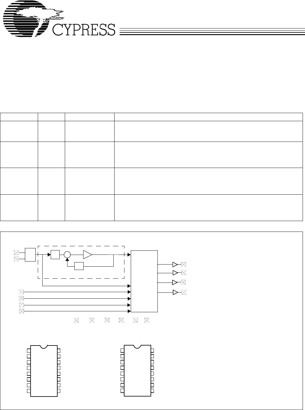
CY24206ZXC-4

MediaClock™ DTV, STB Clock Generato
r
CY24206
Cypress Semiconductor Corporation 3901 North First Street San Jose, CA 95134 408-943-2600
Document #: 38-07451 Rev. *B Revised September 27, 2004
Features
Integrated phase-locked loop (PLL)
Low-jitter, high-accuracy outputs
3.3V operation
Available in 16-pin TSSOP Package
Benefits
•Internal PLL with up to 400-MHz internal operation
Meets critical timing requirements in complex system
designs
Enables application compatibility
Part Number Outputs Input Frequency Output Frequency Range
CY24206-1 3 27 MHz 1 copy 27-MHz reference clock output
1 copy of 81-/81.081-/74.175-/74.250-MHz (frequency selectable)
1 copy of 27-/27.027-/24.725-/24.75-MHz (frequency selectable)
CY24206-2 4 27 MHz 1 copy 27-MHz reference clock output
1 copy of 81-/81.081-/74.175-/74.250-MHz (frequency selectable)
1 copy of 27-/27.027-/24.725-/24.75-MHz (frequency selectable)
1 copy of 27-/27.027-/74.175-/74.25-MHz (frequency selectable)
CY24206-3 4 27 MHz 1 copy 27-MHz reference clock output
1 copy of 81-/81.081-/74.17582-/74.250-MHz (frequency selectable)
1 copy of 27-/27.027-/24.725-/24.75-MHz (frequency selectable)
1 copy of 27-/27.027-/74.175-/74.25-MHz (frequency selectable)
CY24206-4 4 27 MHz 1 copy 27-MHz reference clock output
1 copy of 81-/81.081-/74.17582-/74.250-MHz (frequency selectable)
1 copy of 27-/27.027-/24.725-/24.75-MHz (frequency selectable)
1 copy of 27-/27.027-/74.175-/74.25-MHz (frequency selectable)
XIN
XOUT
OUTPUT
MULTIPLEXER
AND
DIVIDERS
PLL
OSC.
CLK1
Q
P
VCO
VDDL
AVSS
Φ
AVDD
VSS
FS0
FS1
CLK2
REFCLK
16-pin TSSOP
1
2
3
4
5
6
7
8
9
10
11
12
13
14
15
16
VSS
VSSL
FS0
XIN
XOUT
VDD
OE
AVSS
REFCLK
FS2
FS1
AVDD
VDDL
N/C
CLK1
CLK2
FS2
OE
CY24206-1
CLK3 (-2, -3,-4)
16-pin TSSOP
1
2
3
4
5
6
7
8
9
10
11
12
13
14
15
16
VSS
VSSL
FS0
XIN
XOUT
VDD
OE
AVSS
REFCLK
FS2
FS1
AVDD
VDDL
CLK3
CLK1
CLK2
CY24206-2,3,4
Pin Configurations
VDD
VSSL
Logic Block Diagram
[+] Feedback
CY24206
Document #: 38-07451 Rev. *B Page 2 of 6
Frequency Select Options
FS2 FS1 FS0 CLK1 (-1,-2) CLK1 (-3,-4) CLK2 CLK3 (-2, -3,-4) REFCLK Units
0 0 0 81 81 27 (CLK1/3) 27 (CLK1/3) 27 MHz
0 0 1 81.081 81.081 27.027 (CLK1/3) 27.027 (CLK1/3) 27 MHz
0 1 0 74.175 74.17582 24.725 (CLK1/3) 74.17582 (CLK1) 27 MHz
0 1 1 74.250 74.25 24.75 (CLK1/3) 74.25 (CLK1) 27 MHz
1 0 0 81 81 27 27 (CLK1/3) 27 MHz
1 0 1 81.081 81.081 27 27.027 (CLK1/3) 27 MHz
1 1 0 74.175 74.1758 27 74.175 (CLK1) 27 MHz
1 1 1 74.250 74.25 27 74.25 (CLK1) 27 MHz
Pin Description
Name Pin Number Description
XIN 1 Reference Crystal Input.
V
DD
2 Voltage Supply.
AV
DD
3 Analog Voltage Supply.
OE 4 Output Enable, weak internal pull-up. 0 = outputs off, 1 = outputs on.
AV
SS
5 Analog Ground.
V
SSL
6 VDDL Ground.
CLK1 (-1,-2) 7 81-/81.081-/74.175-/74.250-MHz Clock Output (frequency selectable).
CLK1 (-3,-4) 7 81-/81.081-/74.17582-/74.25-MHz Clock Output (frequency selectable).
CLK2 8 27-/27.027-/24.725-/24.75-MHz Clock Output (frequency selectable).
REFCLK 9 Reference Clock Output.
FS0 10 Frequency Select 0, weak internal pull-up.
V
DDL
11 Voltage Supply.
N/C (-1) 12 No Connect.
CLK3 (-2,-3,-4) 12 27-/27.027-/74.175-/74.25-MHz Clock Output (frequency selectable).
VSS 13 Ground.
FS1 14 Frequency Select 1, weak internal pull-up.
FS2 15 Frequency Select 2, weak internal pull-up.
XOUT 16 Reference Crystal Output.
[+] Feedback
CY24206
Document #: 38-07451 Rev. *B Page 3 of 6
Test and Measurement Set-up
Note:
1. Not 100% tested.
Absolute Maximum Conditions
Parameter Description Min. Max. Unit
V
DD
Supply Voltage –0.5 7.0 V
V
DDL
I/O Supply Voltage 7.0 V
T
J
Junction Temperature 125 °C
Digital Inputs AV
SS
– 0.3 AV
DD
+ 0.3 V
Electrostatic Discharge 2 kV
Recommended Operating Conditions
Parameter Description Min. Typ. Max. Unit
V
DD
/AV
DDL
/V
DDL
Operating Voltage 3.135 3.3 3.465 V
T
A
Ambient Temperature 0 70 °C
C
LOAD
Max. Load Capacitance 15 pF
f
REF
Reference Frequency 27 MHz
DC Electrical Specifications
Parameter
[1]
Name Description Min. Typ. Max. Unit
I
OH
Output High Current V
OH
= V
DD
– 0.5, V
DD
/V
DDL
= 3.3V 12 24 mA
I
OL
Output Low Current V
OL
= 0.5, V
DD
/V
DDL
= 3.3V 12 24 mA
I
IH
Input High Current V
IH
= V
DD
–510µA
I
IL
Input Low Current V
IL
= 0V 50 µA
V
IH
Input High Voltage CMOS levels, 70% of V
DD
0.7 VDD
V
IL
Input Low Voltage CMOS levels, 30% of V
DD
0.3 VDD
I
VDD
Supply Current AV
DD
/V
DD
Current 25 mA
I
VDDL
Supply Current V
DDL
Current 20 mA
R
UP
Pull-up resistor on Inputs V
DD
= 3.14 to 3.47V, measured V
IN
= 0V 100 150 k
AC Electrical Specifications
Parameter
[1]
Name Description Min. Typ. Max. Unit
DC Output Duty Cycle Duty Cycle is defined in Figure 1; t1/t2, 50% of
V
DD
45 50 55 %
ER Rising Edge Rate Output Clock Edge Rate, Measured from 20% to
80% of V
DD
, C
LOAD
= 15 pF. See Figure 2.
0.8 1.4 V/ns
EF Falling Edge Rate Output Clock Edge Rate, Measured from 80% to
20% of V
DD
, C
LOAD
= 15 pF. See Figure 2.
0.8 1.4 V/ns
t
9
Clock Jitter CLK1, CLK2 Peak-Peak period jitter 200 ps
t
10
PLL Lock Time 3ms
0.1 µF
V
DDs
Outputs
C
LOAD
GND
DUT
[+] Feedback

CY24206ZXC-4

Mfr. #:
Manufacturer:
Cypress Semiconductor
Description:
Phase Locked Loops - PLL MediaClock Clock COM
Lifecycle:
New from this manufacturer.
Delivery:
DHL FedEx Ups TNT EMS
Payment:
T/T Paypal Visa MoneyGram Western Union

Products related to this Datasheet