LT3652HV
13
3652hvfb
For more information www.linear.com/LT3652HV
APPLICATIONS INFORMATION
In low V
IN
applications, the BOOST supply can be powered
by an external source for start-up, eliminating the V
IN
start-up requirement.
V
BAT
Output Decoupling
An LT3652HV charger output requires bypass capacitance
connected from the BAT pin to ground (C
BAT
). A 10µF
ceramic capacitor is required for all applications. In systems
where the battery can be disconnected from the charger
output, additional bypass capacitance may be desired for
visual indication for a no-battery condition (see the Status
Pins section).
If it is desired to operate a system load from the LT3652HV
charger output when the battery is disconnected, additional
bypass capacitance is required. In this type of application,
excessive ripple and/or low amplitude oscillations can oc
-
cur without additional output bulk capacitance. For these
applications, place a 100µF low ESR non-ceramic capacitor
(chip tantalum or organic semiconductor capacitors such
as Sanyo OS-CONs or POSCAPs) from BAT to ground,
in parallel with the 10µF ceramic bypass capacitor. This
additional bypass capacitance may also be required in
systems where the battery is connected to the charger
with long wires. The voltage rating of C
BAT
must meet or
exceed the battery float voltage.
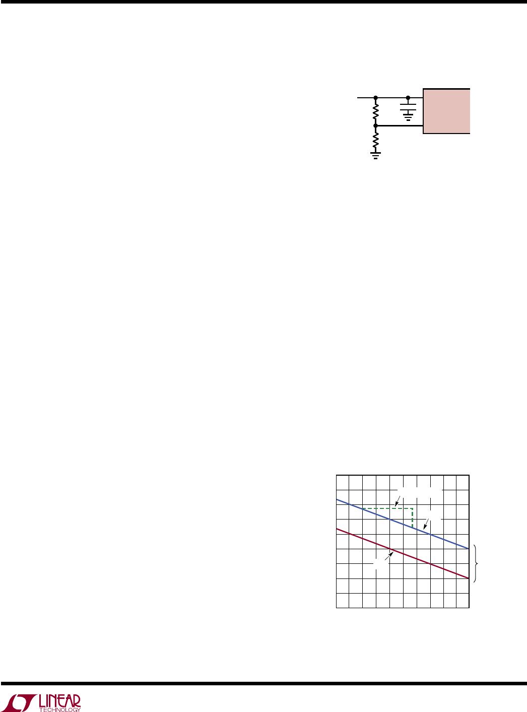
Inductor Selection
The primary criterion for inductor value selection in an
LT3652HV charger is the ripple current created in that
inductor. Once the inductance value is determined, an
inductor must also have a saturation current equal to or
exceeding the maximum peak current in the inductor. An
inductor value (L), given the desired amount of peak-to-
peak inductor ripple current (ΔI
L
) can be approximated
using the relation:
L =
10 R
SENSE
ΔI
L
I
CHG(MAX)
V
BAT(FLT)
1–
V
BAT(FLT)
V
IN(MAX)
µH
( )
In the above relation, V
IN(MAX)
is the maximum operational
voltage. Ripple current is typically set within a range of
25% to 35% of I
CHG(MAX)
, so an inductor value can be
determined by setting 0.25 < ΔI
L
/I
CHG(MAX)
< 0.35.
Figure 3. 14.4V at 1.5A Switched Inductor Values
MAXIMUM OPERATIONAL V
IN
VOLTAGE (V)
18 20 22
4
SWITCHED INDUCTOR VALUE (µH)
12
10
14
24
16
18
20
22
34
3652 F03
8
6
26 2824 30 32
Magnetics vendors typically specify inductors with maxi-
mum RMS and saturation current ratings. Select an inductor
that has a saturation current rating at or above I
CHG(MAX)
+ ∆I
L
/I
CHG(MAX)
, and an RMS rating above I
CHG(MAX)
. In-
ductors must also meet a maximum volt-second product
requirement. If this specification is not in the data sheet of
an inductor, consult the vendor to make sure the maximum
volt-second product is not being exceeded by your design.
The minimum required volt-second product is:
V
BAT(FLT)
1
V
BAT(FLT)
V
IN(MAX)
V µS
( )
Rectifier Selection
The rectifier diode from SW to GND, in a LT3652HV battery
charger provides a current path for the inductor current
when the main power switch is disabled. The rectifier is
selected based upon forward voltage, reverse voltage, and
maximum current. A Schottky diode is required, as low
forward voltage yields the lowest power loss and highest
efficiency. The rectifier diode must be rated to withstand
reverse voltages greater than the maximum V
IN
voltage.
LT3652HV
14
3652hvfb
For more information www.linear.com/LT3652HV
APPLICATIONS INFORMATION
The minimum average diode current rating (I
DIODE(MAX)
)
is calculated with maximum output current (I
CHG(MAX)
),
maximum operational V
IN
, and output at the precondition
threshold (V
BAT(PRE)
, or 0.7 • V
BAT(FLT)
):
I
DIODE(MAX)
>I
CHG(MAX)
V
IN(MAX)
V
BAT(PRE)
V
IN(MAX)
(A)
For example, a rectifier diode for a 7.2V, 2A charger with
a 25V maximum input voltage would require:
I
DIODE(MAX)
> 2 A
25V
0.7(7.2V)
25V
,or
I
DIODE(MAX)
>1.6A
Battery Float Voltage Programming
The output battery float voltage (V
BAT(FLT)
) is programmed
by connecting a resistor divider from the BAT pin to V
FB
.
V
BAT(FLT)
can be programmed up to 18V.
Figure 4. Feedback Resistors from BAT to V
FB
Program Float Voltage
BAT
+
V
FB
R
FB2
R
FB1
LT3652HV
3652 F04
Because the battery voltage is across the V
BAT(FLT)
pro-
gramming resistor divider, this divider will draw a small
amount of current from the battery (I
RFB
) at a rate of:
I
RFB
= 3.3/R
FB2
Precision resistors in high values may be hard to ob-
tain, so for some lower V
BAT(FLT)
applications, it may be
desirable to use smaller-value feedback resistors with an
additional resistor (R
FB3
) to achieve the required 250k
equivalent resistance. The resulting 3-resistor network,
as shown in Figure 5, can ease component selection
and/or increase output voltage precision, at the expense of
additional current through the feedback divider.
For a three-resistor network, R
FB1
and R
FB2
follow the
relation:
R
FB2
/R
FB1
= 3.3/(V
BAT(FLT)
– 3.3)
Example:
For V
BAT(FLT)
= 3.6V:
R
FB2
/R
FB1
= 3.3/(3.6 - 3.3) = 11.
Setting divider current (I
RFB
) = 10µA yields:
R
FB2
= 3.3/10µA
R
FB2
= 330k
Solving for R
FB1
:
R
FB1
= 330k/11
R
FB1
= 30k
The divider equivalent resistance is:
R
FB1
||R
FB2
= 27.5k
BAT
+
V
FB
R
FB2
R
FB3
R
FB1
LT3652HV
3652 F05
Figure 5. A Three-Resistor Feedback Network Can
Ease Component Selection
Using a resistor divider with an equivalent input resistance
at the V
FB
pin of 250k compensates for input bias current
error. Required resistor values to program desired V
BAT(FLT)
follow the equations:
R
FB1
= (V
BAT(FLT)
• 2.5 • 10
5
)/3.3 (Ω)
R
FB2
= (R
FB1
• (2.5 • 10
5
))/(R
FB1
- (2.5 • 10
5
)) (Ω)
The charge function operates to achieve the final float
voltage of 3.3V on the V
FB
pin. The auto-restart feature
initiates a new charging cycle when the voltage at the V
FB
pin falls 2.5% below that float voltage.
LT3652HV
15
3652hvfb
For more information www.linear.com/LT3652HV
To satisfy the 250k equivalent resistance to the V
FB
pin:
R
FB3
= 250k − 27.5k
R
FB3
= 223k.
Because the V
FB
pin is a relatively high impedance node,
stray capacitances at this pin must be minimized. Spe
-
cial attention should be given to any stray capacitances
that can couple external signals onto the pin, which can
produce undesirable output transients or ripple. Effects of
parasitic capacitance can typically be reduced by adding
a small-value (20pF to 50pF) feedforward capacitor from
the BAT pin to the V
FB
pin.
Extra care should be taken during board assembly. Small
amounts of board contamination can lead to significant
shifts in output voltage. Appropriate post-assembly board
cleaning measures should be implemented to prevent
board contamination, and low-leakage solder flux is
recommended.
Input Supply Voltage Regulation
The LT3652HV contains a voltage monitor pin that enables
programming a minimum operational voltage. Connect
-
ing a resistor divider from V
IN
to the V
IN_REG
pin enables
programming of minimum input supply voltage, typically
used to program the peak power voltage for a solar panel.
Maximum charge current is reduced when the V
IN_REG
pin
is below the regulation threshold of 2.7V.
If an input supply cannot provide enough power to satisfy
the requirements of an LT3652HV charger, the supply volt
-
age will collapse. A minimum operating supply voltage can
thus be programmed by monitoring the supply through
a resistor divider, such that the desired minimum voltage
corresponds to 2.7V at the V
IN_REG
pin. The LT3652HV
servos the maximum output charge current to maintain
the voltage on V
IN_REG
at or above 2.7V.
Programming of the desired minimum voltage is ac
-
complished by connecting a resistor divider as shown in
Figure 6. The ratio of R
IN1
/R
IN2
for a desired minimum
voltage (V
IN(MIN)
) is:
R
IN1
/R
IN2
= (V
IN(MIN)
/2.7) – 1
APPLICATIONS INFORMATION
If the voltage regulation feature is not used, connect the
V
IN_REG
pin to V
IN
.
MPPT Temperature Compensation
A typical solar panel is comprised of a number of series-con
-
nected cells, each cell being a forward-biased p-n junction.
As such, the open-circuit voltage (V
OC
) of a solar cell has
a temperature coefficient that is similar to a common p-n
diode, or about –2mV/°C. The peak power point voltage
(V
MP
) for a crystalline solar panel can be approximated as
a fixed voltage below V
OC
, so the temperature coefficient
for the peak power point is similar to that of V
OC
.
Panel manufacturers typically specify the 25°C values for
V
OC
, V
MP
, and the temperature coefficient for V
OC
, making
determination of the temperature coefficient for V
MP
of a
typical panel straight forward.
The LT3652HV employs a feedback network to program
the V
IN
input regulation voltage. Manipulation of the
network makes for efficient implementation of various
temperature compensation schemes for a maximum peak
Figure 6. Resistor Divider Sets Minimum V
IN
V
IN
V
IN_REG
R
IN2
R
IN1
LT3652HV
INPUT
SUPPLY
3652 F06
Figure 7. Temperature Characteristics for Solar Panel
Output Voltage
TEMPERATURE (°C)
5
PANEL VOLTAGE (V)
25
45
55
15 35
3652 F07
V
OC(25°C)
V
MP(25°C)
V
MP
V
OC
V
OC
TEMP CO.
V
OC
– V
MP

LT3652HVEMSE#PBF

Mfr. #:
Manufacturer:
Analog Devices / Linear Technology
Description:
Battery Management Pwr Track 2A Bat Chr
Lifecycle:
New from this manufacturer.
Delivery:
DHL FedEx Ups TNT EMS
Payment:
T/T Paypal Visa MoneyGram Western Union