NXP Semiconductors
BTA316X-800C
3Q Hi-Com Triac
BTA316X-800C All information provided in this document is subject to legal disclaimers. © NXP Semiconductors N.V. 2014. All rights reserved
Product data sheet 19 June 2014 6 / 13
9. Thermal characteristics
Table 6. Thermal characteristics
Symbol Parameter Conditions Min Typ Max Unit
full cycle or half cycle; with heatsink
compound; Fig. 6
- - 4 K/WR
th(j-h)
thermal resistance
from junction to
heatsink
full cycle or half cycle; without heatsink
compound; Fig. 6
- - 5.5 K/W
R
th(j-a)
thermal resistance
from junction to
ambient
in free air - 55 - K/W
003aab672
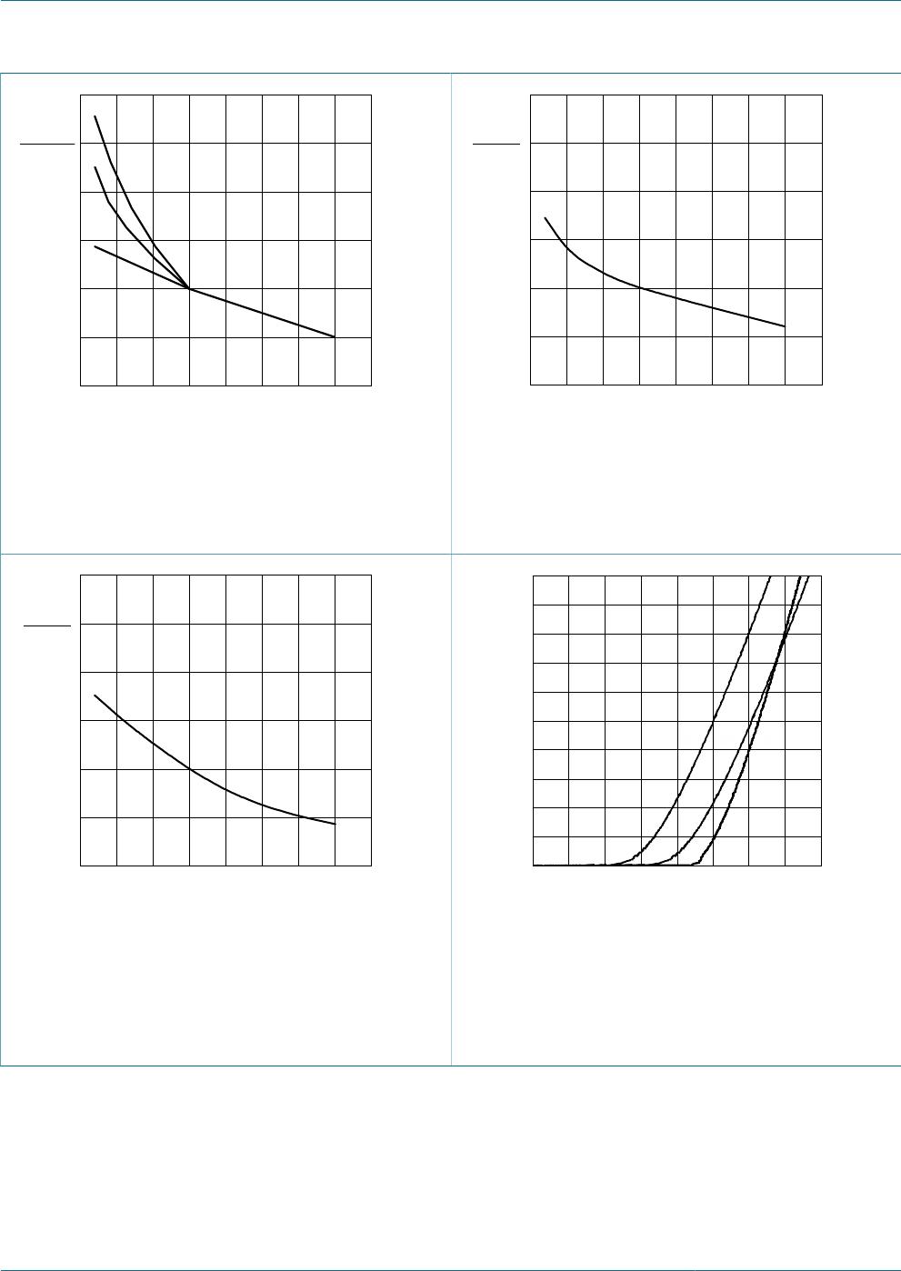
10
-1
10
-2
1
10
Z
th(j-h)
(K/W)
10
-3
t
p
(s)
10
-5
1 1010
-1
10
-2
10
-4
10
-3
(1)
(2)
(3)
(4)
t
p
P
t
(1) Unidirectional (half cycle) without heatsink compound
(2) Unidirectional (half cycle) with heatsink compound
(3) Bidirectional (full cycle) without heatsink compound
(4) Bidirectional (full cycle) with heatsink compound
Fig. 6. Transient thermal impedance from junction to heatsink as a function of pulse duration
10. Isolation characteristics
Table 7. Isolation characteristics
Symbol Parameter Conditions Min Typ Max Unit
V
isol(RMS)
RMS isolation voltage from all terminals to external heatsink;
sinusoidal waveform; clean and dust
free; 50 Hz ≤ f ≤ 60 Hz; RH ≤ 65 %;
T
h
= 25 °C
- - 2500 V
C
isol
isolation capacitance from main terminal 2 to external
heatsink; f = 1 MHz; T
h
= 25 °C
- 10 - pF