Working Peak Reverse Voltage:5.0-190 Volts
Peak Pulse Power:200 Watts
RoHS Device
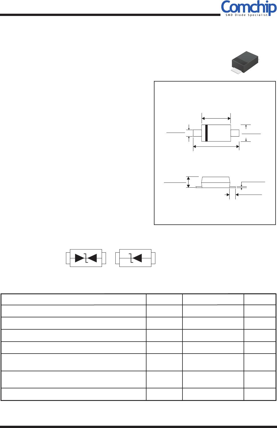
Dimensions in inches and (millimeter)
SOD-123
0.053 (1.33)
0.037 (0.93)
0.01 (0.25)min
0.008 (0.20)max
0.152 (3.82)
0.140 (3.51)
0.071 (1.78)
0.055 (1.38)
0.112 (2.81)
0.100 (2.51)
0.044 (1.09)
0.031 (0.77)
Notes:
2. Measured on 8.3ms single half sine-wave or equivalent square wave, duty cycle=4 pulses per minute maximum.
SMD Transient Voltage Suppressor
Page 1
AQW-JTV05
REV:A
Comchip Technology CO., LTD.
ATV02W5V0-HF Thru ATV02W191-HF
Halogen Free
1. Non-repetitive current pulse, per Fig.3 and derated above TA=25°C per Fig.1
3. Company reserves the right to improve product design , functions and reliability without notice.
Features
- Glass passivated chip.
- Low leakage current.
- 200W peak pulse power capability with a 10/1000µs
waveform, repetitive rate (duty cycle):0.01%.
- Uni and bidirectional unit.
- Excellent clamping capability.
- Very fast response time.
Mechanical data
- Case: Molded plastic.
- Epoxy: UL 94V-0 rate flame retardant.
- Lead: Solderable per MIL-STD-750, method 2026.
- Polarity: Color band denotes cathode end
except bipolar.
- Mounting position: Any.
Parameter
Symbol
Value
Unit
Maximum Rating and Electrical Characteristics
Power dissipation on infinite heatsink at TL = 75°C
0.4
PD W
200
W
PPP
Peak power dissipation at 10/1000µs waveform (Note 1)
1000
W
PPP
Peak power dissipation at 8/20µs waveform (Note 1)
Peak forward surge current, 8.3ms single half sone-wave
undirestional only (Note 2)
20
IFSM
A
A
Peak pulse current with a 10/1000µs waveform (Note 1)
See next tableIPP
Operating junction and storage temperature range
-55 to +150
TJ,TSTG
°C
Ratings at 25°C ambient temperature unless otherwise specified.
Single phase, half wave, 60Hz, resistive or inductive load.
For capacitive load, derate current by 20%.
Max.instantaneous forward voltage at 25A for
undirestional only
VF
3.5
V
- Weight: 0.016 grams .(approx)
Circuit Diagram
Uni-directional
Bi-directional
- Comply with AEC-Q101

