DG611E, DG612E, DG613E
www.vishay.com
Vishay Siliconix
S17-0578-Rev. A, 24-Apr-17
1
Document Number: 78910
For technical questions, contact: analogswitchtechsupport@vishay.com
THIS DOCUMENT IS SUBJECT TO CHANGE WITHOUT NOTICE. THE PRODUCTS DESCRIBED HEREIN AND THIS DOCUMENT
ARE SUBJECT TO SPECIFIC DISCLAIMERS, SET FORTH AT www.vishay.com/doc?91000
1.4 pC Charge Injection, 100 pA Leakage, Quad SPST Switches
DESCRIPTION
The DG611E, DG612E, and DG613E contain four
independently selectable SPST switches. They offer
improved performance over the industry standard DG611
series. The DG611E and DG612E have all switches normally
closed and normally open respectively, while the DG613E
has 2 normally open and 2 normally closed switches.
They are designed to operate from a 3 V to 12 V single
supply or from ± 3 V to ± 5 V dual supplies and are fully
specified at +3 V, +5 V and ± 5 V. All control logic inputs
have guaranteed 2 V logic high limits when operating from
+5 V or ± 5 V supplies and 1.4 V when operating from a
+3 V supply.
The DG611E, DG612E, and DG613E switches conduct
equally well in both directions and offer rail to rail analog
signal handling.
1.4 pC low charge injection, coupled with very low switch
capacitance: 3 pF, fast switching speed: t
on
/t
off
23 ns/14 ns
and excellent 3 dB bandwidth: 1 GHz, make these products
ideal for precision instrumentation, high-end data
acquisition, automated test equipment and high speed
communication applications.
Operation temperature is specified from -40 °C to +125 °C.
The DG611E, DG612E, and DG613E are available in 16 lead
SOIC, TSSOP and the space saving 1.8 mm x 2.6 mm
miniQFN packages.
FEATURES
• Low charge injection (1.4 pC typ.)
• Leakage current < 0.25 nA at 85 °C
• Low switch capacitance (C
soff
3 pF typ.)
•Low R
DS(on)
- 115 max.
• Fully specified with single supply operation at
3 V, 5 V, and dual supplies at ± 5 V
• Low voltage, 2.5 V CMOS/TTL compatible
• 1 GHz, 3 dB bandwidth
• Excellent isolation performance (-59 dB at 10 MHz)
• Excellent crosstalk performance (-74 dB at 10 MHz)
•
Fully specified from -40 °C to +85 °C and -40 °C to +125 °C
• 16 lead SOIC, TSSOP and miniQFN package
(1.8 mm x 2.6 mm)
• Material categorization: for definitions of compliance
please see www.vishay.com/doc?99912
APPLICATIONS
• Precision instrumentation
• Medical instrumentation
• Automated test equipment
• High speed communications applications
• High-end data acquisition
• Sample and hold applications
• Sample and hold systems
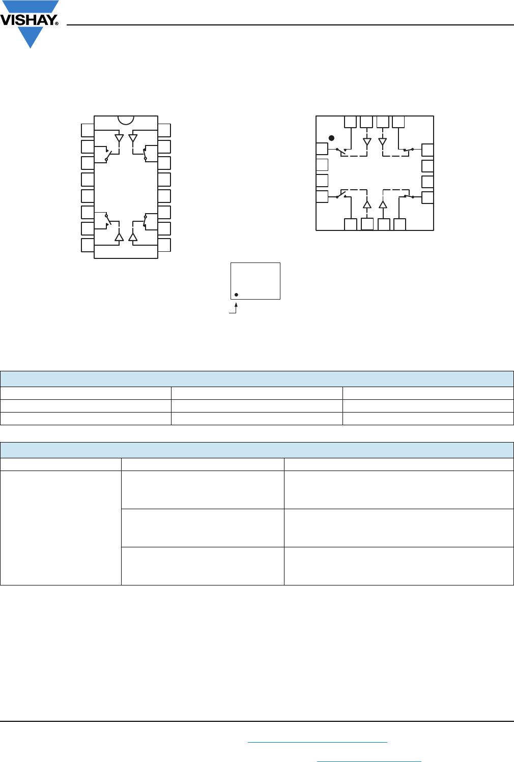
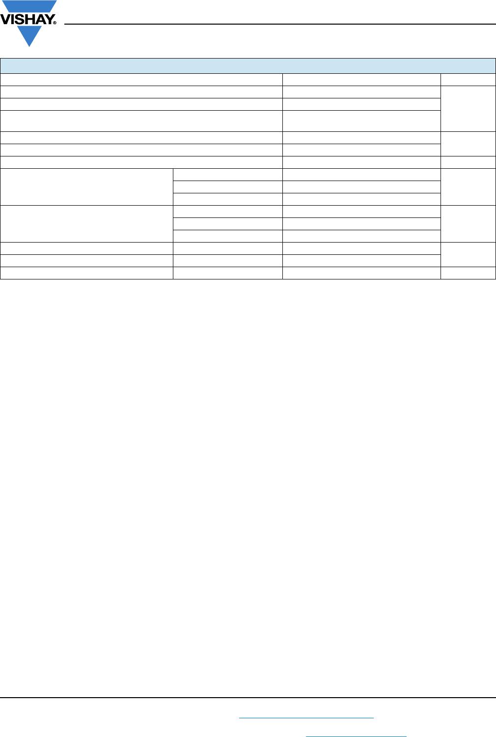
FUNCTIONAL BLOCK DIAGRAM AND PIN CONFIGURATION
TRUTH TABLE
LOGIC DG611E DG612E
0OnOff
1OffOn
DG611E
SOIC/TSSOP
Top View
S
2
V+
NC
S
3
IN
3
D
3
D
4
IN
4
IN
2
D
2
D
1
IN
1
S
1
V-
GND
S
4
1
2
3
4
5
6
8
7
16 15 14 13
12
11
10
9
1
2
3
4
5
6
7
8
16
15
14
13
12
11
10
9
Top View
IN
1
IN
2
D
1
D
2
S
1
S
2
V-
V+
GND
NC
S
4
S
3
D
4
D
3
IN
4
IN
3
DG611E
miniQFN
Pin 1
Device Marking: Txx for DG611E
(miniQFN16) Uxx for DG612E
Vxx for DG613E
xx = Date/Lot Traceability Code
Txx