DG611E, DG612E, DG613E
www.vishay.com
Vishay Siliconix
S17-0578-Rev. A, 24-Apr-17
10
Document Number: 78910
For technical questions, contact: analogswitchtechsupport@vishay.com
THIS DOCUMENT IS SUBJECT TO CHANGE WITHOUT NOTICE. THE PRODUCTS DESCRIBED HEREIN AND THIS DOCUMENT
ARE SUBJECT TO SPECIFIC DISCLAIMERS, SET FORTH AT www.vishay.com/doc?91000
TEST CIRCUITS
Fig. 1 - Switching Time
Fig. 2 - Break-Before-Make (DG613E)
Fig. 3 - Charge Injection
0 V
Logic
Input
Switch
Input*
3 V
50 %
0 V
V
S
t
r
< 5 ns
t
f
< 5 ns
90 %
t
OFF
t
ON
V
O
Note: Logic input waveform is inverted for switches that
have the opposite logic sense control
C
L
(includes fixture and stray capacitance)
V+
IN
R
L
R
L
+ r
DS(on)
V
O
= V
S
S D
- 5 V
V
O
GND
C
L
35 pF
V-
R
L
300 Ω
+ 5 V
90 %
V
S
0 V
Logic
Input
Switch
Switch
Output
3 V
50 %
0 V
Output
0 V
90 %
V
O2
V
O1
90 %
V
S1
V
S2
t
D
t
D
V
O2
C
L
(includes fixture and stray capacitance)
V+
S
2
V-
S
1
V
S2
IN
2
D
2
V
S1
R
L2
300 Ω
D
1
V
O1
C
L2
35 pF
-5 V
GND
+ 5 V
R
L1
300 Ω
C
L1
35 pF
IN
1
C
L
1 nF
D
R
g
V
O
V+
S
V-
3 V
IN
V
g
- 5 V
GND
+ 5 V
OFFONOFF
OFFONOFF
V
O
ΔV
O
IN
X
IN
X
Q = ΔV
O
x C
L
DG611E, DG612E, DG613E
www.vishay.com
Vishay Siliconix
S17-0578-Rev. A, 24-Apr-17
11
Document Number: 78910
For technical questions, contact: analogswitchtechsupport@vishay.com
THIS DOCUMENT IS SUBJECT TO CHANGE WITHOUT NOTICE. THE PRODUCTS DESCRIBED HEREIN AND THIS DOCUMENT
ARE SUBJECT TO SPECIFIC DISCLAIMERS, SET FORTH AT www.vishay.com/doc?91000
TEST CIRCUITS
Fig. 4 - Crosstalk
Fig. 5 - Off-Isolation Fig. 6 - Source / Drain Capacitances
Vishay Siliconix maintains worldwide manufacturing capability. Products may be manufactured at one of several qualified locations. Reliability data for Silicon
Technology and Package Reliability represent a composite of all qualified locations. For related documents such as package / tape drawings, part marking, and
reliability data, see www.vishay.com/ppg?78910
.
0 V, 2.4 V
S
1
X
TALK
Isolation = 20 log
V
O
V
S
D
2
C = RF bypass
R
L
D
1
S
2
V
S
0 V, 2.4 V
IN
1
50 Ω
V
O
IN
2
R
g
= 50 Ω
V+
- 5 V
GND V -
NC
C
+ 5 V
C
R
L
50 Ω
D
0 V, 2.4 V
V+
R
g
= 50 Ω
- 5 V
GND V-
C
V
S
Off Isolation = 20 log
V
O
V
S
IN
V
O
+ 5 V
S
C
C = RF Bypass
D
IN
S
V+
-5 V
GND V -
C
0 V, 2.4 V
Meter
HP4192A
Impedance
Analyzer
or Equivalent
+ 5 V
C
Package Information
www.vishay.com
Vishay Siliconix
Revision: 09-May-16
1
Document Number: 64694
For technical questions, contact: analogswitchtechsupport@vishay.com
THIS DOCUMENT IS SUBJECT TO CHANGE WITHOUT NOTICE. THE PRODUCTS DESCRIBED HEREIN AND THIS DOCUMENT
ARE SUBJECT TO SPECIFIC DISCLAIMERS, SET FORTH AT www.vishay.com/doc?91000
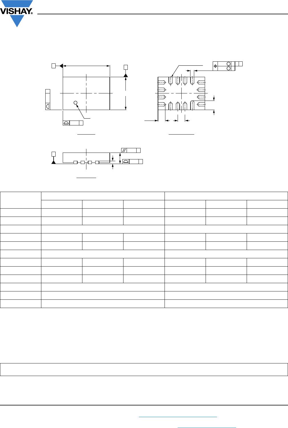
Thin miniQFN16 Case Outline
Notes
(1)
Use millimeters as the primary measurement.
(2)
Dimensioning and tolerances conform to ASME Y14.5M. - 1994.
(3)
N is the number of terminals. Nd and Ne is the number of terminals in each D and E site respectively.
(4)
Dimensions b applies to plated terminal and is measured between 0.15 mm and 0.30 mm from terminal tip.
(5)
The pin 1 identifier must be existed on the top surface of the package by using identification mark or other feature of package body.
(6)
Package warpage max. 0.05 mm.
DIMENSIONS
MILLIMETERS
(1)
INCHES
MIN. NOM. MAX. MIN. NOM. MAX.
A 0.50 0.55 0.60 0.020 0.022 0.024
A1 0 - 0.05 0 - 0.002
A3 0.15 ref. 0.006 ref.
b 0.15 0.20 0.25 0.006 0.008 0.010
D 2.50 2.60 2.70 0.098 0.102 0.106
e 0.40 BSC 0.016 BSC
E1.70
1.80 1.90
0.067
0.071 0.075
L 0.35 0.40 0.45 0.014 0.016 0.018
L1 0.45 0.50 0.55 0.018 0.020 0.022
N
(3)
16 16
Nd
(3)
44
Ne
(3)
44
ECN: T16-0226-Rev. B, 09-May-16
DWG: 6023
0.10 C
0.10
A
A3
C
0.10 C
0.10 C
Side view
Top view Bottom view
C
A
B
13
12 11 10
D
E
9
8
7
6
5
8
7
6
5
13
14
15
16
L1
1234
Pin #1 identier
(5)
Seating
plane
Terminal tip
(4)
16 x b
0.10
0.05
C
C
M
M
AB
1211109
4
15 x L
321
e
14
15
16

DG613EEQ-T1-GE4

Mfr. #:
Manufacturer:
Vishay / Siliconix
Description:
Analog Switch ICs Quad SPST 1.4pC 16-pin TSSOP
Lifecycle:
New from this manufacturer.
Delivery:
DHL FedEx Ups TNT EMS
Payment:
T/T Paypal Visa MoneyGram Western Union