ADL5545 Data Sheet
Rev. A | Page 14 of 20
APPLICATIONS INFORMATION
BASIC CONNECTIONS
Figure 29 shows the basic connections for operating the
ADL5545. The device supports operation from 30 MHz to 6 GHz.
However, for optimal performance at lower and higher frequency
bands, the board configuration must be adjusted. Table 6 lists
the recommended board configuration to operate the device at
various frequency bands.
RFIN
GND
GND
RFOUT
1
2
(2)
3
ADL5545
L1
V
POS
GND
C7
RFIN
C1
C8
RFOUT
C2
C6
10µF
C5
1nF
C4
100pF
11385-028
Figure 29. Basic Connections
A 5 V dc bias is supplied to the amplifier through the bias
inductor connected to RFOUT (Pin 3). The bias voltage must
be decoupled using 100 pF, 1 nF, and 10 µF power supply
decoupling capacitors. The typical current consumption for
the ADL5545 is 56 mA.
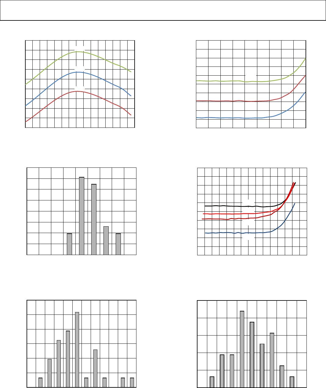
At low and high frequencies, the device exhibits improved
performance with the suggested setup configuration listed in
Table 6. Figure 30 to Figure 33 provide a comparison of the
performance of the device at the 100 MHz to 500 MHz and
4 GHz to 6 GHz bands when driven with the optimal setup
configuration and the default setup configuration.
40
35
0
5
10
15
20
25
30
0.10 0.15
0.20
0.25
0.30 0.35 0.40 0.45 0.50
NOISE FIGURE, GAIN, P1dB, OIP3 (dB, dBm)
FREQUENCY (GHz)
GAIN, DEFAULT SETUP CONFIGURATION
GAIN, LOW FREQUENCY CONFIGURATION
P1dB, DEFAULT SETUP CONFIGURATION
P1dB, LOW FREQUENCY CONFIGURATION
NOISE FIGURE, DEFAULT SETUP CONFIGURATION
NOISE FIGURE, LOW FREQUENCY CONFIGURATION
OIP3, DEFAULT SETUP CONFIGURATION
OIP3, LOW FREQUENCY CONFIGURATION
1
1385-029
Figure 30. Noise Figure, Gain, P1dB, and OIP3 vs. Frequency,
100 MHz to 500 MHz, Comparison of Performance
with the Optimized Settings and the Default Configuration
0
–5
–10
–15
–25
–35
–20
–30
0.10 0.15 0.20
0.25
0.30 0.35 0.40 0.45 0.50
S-PARAMETERS (dB)
FREQUENCY (GHz)
S11, DEFAULT SETUP CONFIGURATION
S12, DEFAULT SETUP CONFIGURATION
S22, DEFAULT SETUP CONFIGURATION
S11, LOW FREQUENCY CONFIGURATION
S12, LOW FREQUENCY CONFIGURATION
S22, LOW FREQUENCY CONFIGURATION
1
1385-030
Figure 31. Return Loss and Reverse Isolation, 100 MHz to 500 MHz,
Comparison of Performance with the Optimized Settings
and the Default Configuration
Table 6. Recommended Components for Basic Connections
Frequency Band
AC Coupling Capacitors (0402) DC Bias Inductor (0603HP)
High Frequency Matching
Capacitors (0402)
C1 C2 L1 C7 C8
100 MHz to 500 MHz 100 nF 100 nF 1000 nH Do not install Do not install
500 MHz to 4 GHz (default) 100 pF 100 pF 100 nH Do not install Do not install
4 GHz to 6 GHz 100 pF 100 pF 12 nH 0.1 pF 0.1 pF