LT5511
3
5511i
ELECTRICAL CHARACTERISTICS
PARAMETER CONDITIONS MIN TYP MAX UNITS
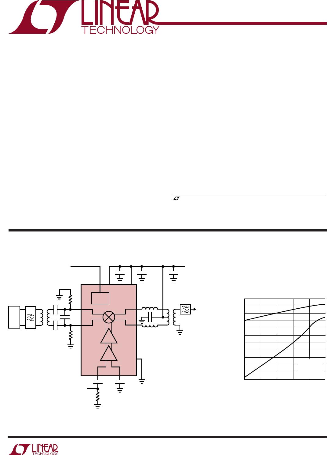
1.9GHz Application: (Test Circuit Shown in Figure 3) V
CC
= 5V
DC
, EN = High, T
A
= 25°C, IF Input = 50MHz at –5dBm, LO Input = 1.95GHz at –10dBm,
RF Output Measured at 1900MHz, unless otherwise noted. (Notes 3, 4)
IF Input Return Loss With External Matching, Z
O
= 50Ω 14 dB
LO Input Power –15 to –5 dBm
LO Input Return Loss With External Matching, Z
O
= 50Ω 11.5 dB
RF Output Return Loss With External Matching, Z
O
= 50Ω 11.5 dB
Conversion Gain –0.7 dB
LO to RF Leakage –47 dBm
Input 1dB Compression 5.2 dBm
Input 3rd Order Intercept Two-Tone, –5dBm/Tone, ∆f = 1MHz 15.5 dBm
Input 2nd Order Intercept Single-Tone, –5dBm 51 dBm
SSB Noise Figure 14 dB
Power Supply Requirements: V
CC
= 5V
DC
, EN = High, T
A
= 25°C, unless otherwise noted.
Supply Voltage 4.0 to 5.25 V
DC
Supply Current 56 65 mA
Shutdown Current (Chip Disabled) EN = Low 1 30 µA
Enable Mode Threshold EN = High 3 V
DC
Disable Mode Threshold EN = Low 0.5 V
DC
Turn ON Time (Note 5) 2 µs
Turn OFF Time (Note 5) 6 µs
Enable Input Current EN = 5V 1 µA
Note 1: Absolute Maximum Ratings are those values beyond which the life
of a device may be impaired.
Note 2: External components on the final test circuit are optimized for
operation at f
RF
= 950MHz, f
LO
= 1GHz and f
IF
= 50MHz (Figure 2).
Note 3: Specifications over the – 40°C to 85°C temperature range are
assured by design, characterization and correlation with statistical process
controls.
Note 4: External components on the final test circuit are optimized for
operation at f
RF
= 1900MHz, f
LO
= 1.95GHz and f
IF
= 50MHz (Figure 3).
Note 5: Turn On and Turn Off times are based on rise and fall times of RF
output envelope from full power to –40dBm with an IF input power of
–5dBm.
Note 6: Part can be used over a broader range of operating frequencies.
Consult factory for applications assistance.