6
LTC3404
3404fb
RUN (Pin 1): Run Control Input. Forcing this pin below
0.4V shuts down the LTC3404. In shutdown all functions
are disabled drawing <1μA supply current. Forcing this
pin above 1.2V enables the LTC3404. Do not leave RUN
floating.
I
TH
(Pin 2): Error Amplifier Compensation Point. The
current comparator threshold increases with this control
voltage. Nominal voltage range for this pin is from 0.5V
to 1.9V.
V
FB
(Pin 3): Feedback Pin. Receives the feedback voltage
from an external resistive divider across the output.
GND (Pin 4): Ground Pin.
SW (Pin 5): Switch Node Connection to Inductor. This pin
connects to the drains of the internal main and synchro-
nous power MOSFET switches.
V
IN
(Pin 6): Main Supply Pin. Must be closely decoupled
to GND, Pin 4.
SYNC/MODE (Pin 7): External Clock Synchronization and
Mode Select Input. To synchronize with an external clock,
apply a clock with a frequency between 1MHz and 1.7MHz.
To select Burst Mode operation, tie to V
IN
. Grounding this
pin selects pulse skipping mode. Do not leave this pin
floating.
PLL LPF (Pin 8): Output of the Phase Detector and Control
Input of Oscillator. Connect a series RC lowpass network
from this pin to ground if externally synchronized. If
unused, this pin may be left open.
UU
U
PI FU CTIO S
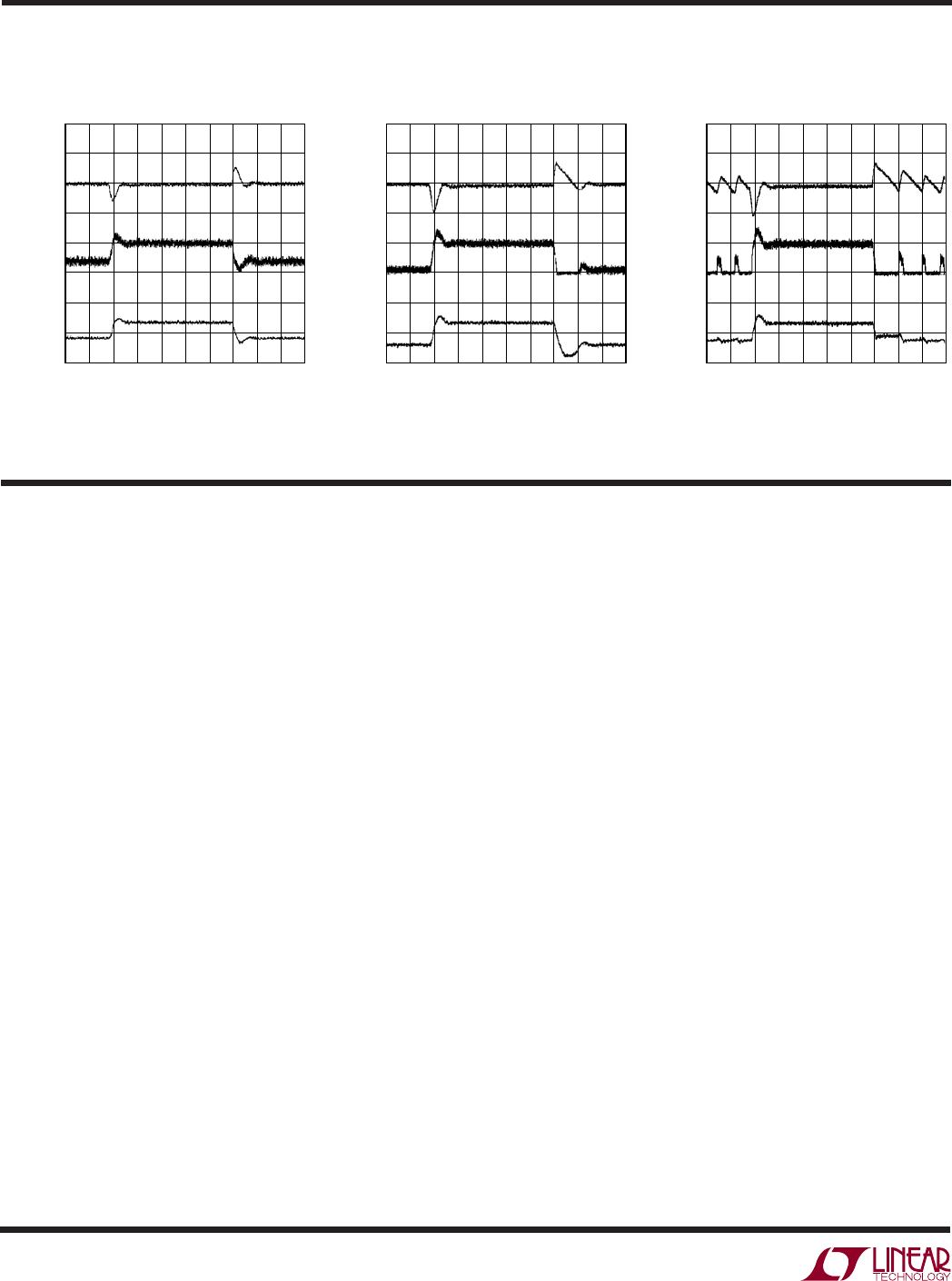
Load Step Response
Load Step Response Load Step Response
40μs/DIV
V
IN
= 3.6V
V
OUT
= 1.5V
L = 4.7μH
C
IN
= 10μF
C
OUT
= 22μF
I
LOAD
= 200mA TO 500mA
PULSE SKIPPING MODE
V
OUT
100mV/DIV
I
L
500mA/DIV
I
TH
1V/DIV
3404 G17
40μs/DIV
V
IN
= 3.6V
V
OUT
= 1.5V
L = 4.7μH
C
IN
= 10μF
C
OUT
= 22μF
I
LOAD
= 50mA TO 500mA
PULSE SKIPPING MODE
V
OUT
100mV/DIV
I
L
500mA/DIV
I
TH
1V/DIV
3404 G18
40μs/DIV
V
IN
= 3.6V
V
OUT
= 1.5V
L = 4.7μH
C
IN
= 10μF
C
OUT
= 22μF
I
LOAD
= 50mA TO 500mA
Burst Mode OPERATION
V
OUT
100mV/DIV
I
L
500mA/DIV
I
TH
1V/DIV
3404 G19
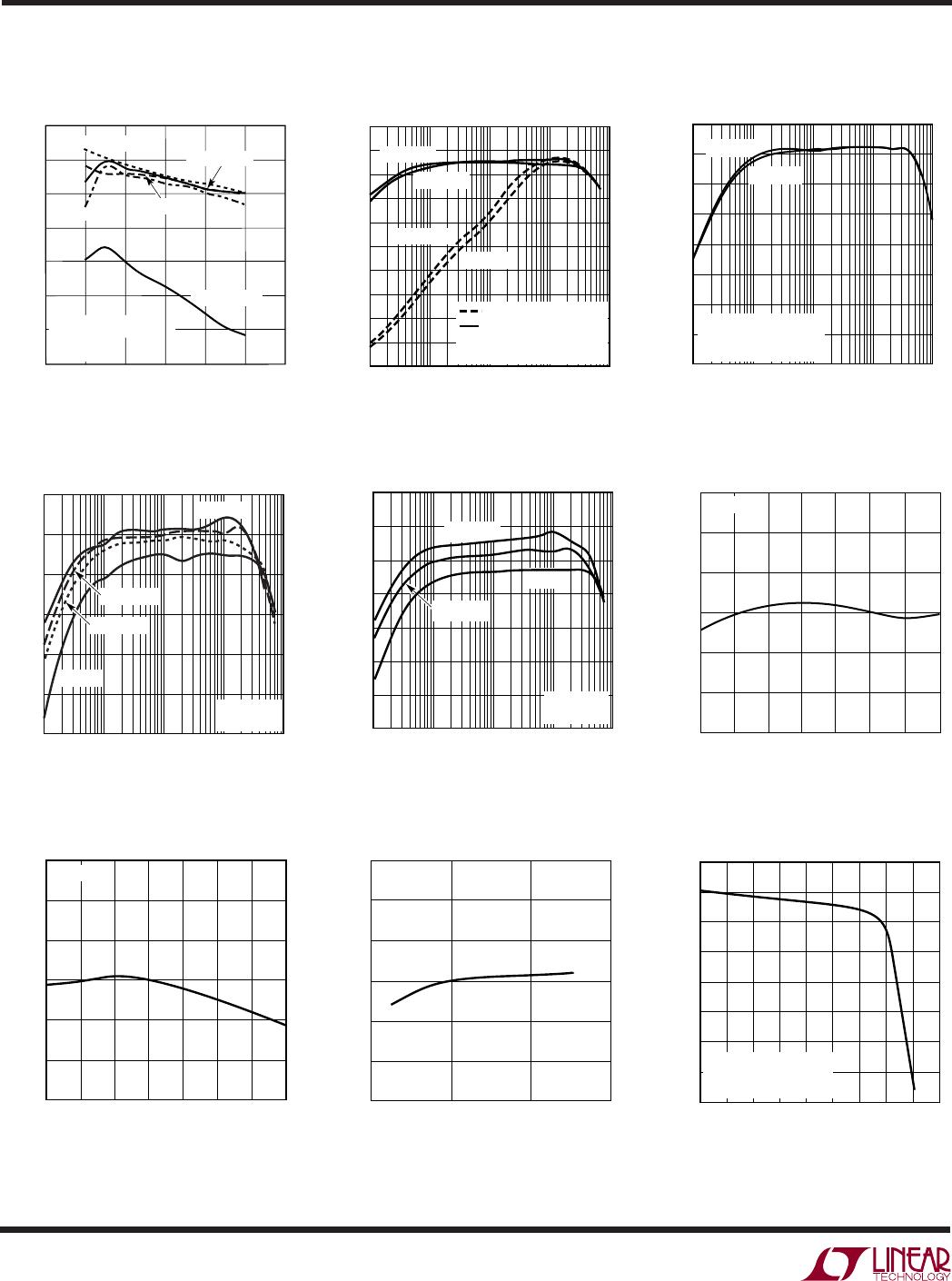
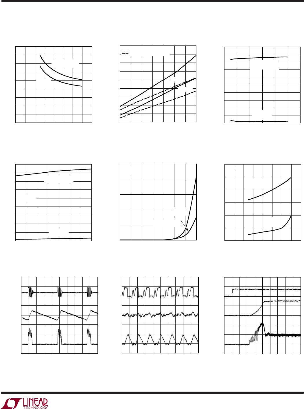
TYPICAL PERFOR A CE CHARACTERISTICS
UW