CRA06S0431K47FTA

Thick Film Resistor Array
www.vishay.com For technical questions, contact: filmresistors.thickfilmchip@vishay.com
Document Number: 31002
252 Revision: 13-Oct-08
CRA06E, CRA06S
Vishay
CRA06E and CRA06S Thick Film resistor arrays are
constructed on a high grade ceramic body with convex
terminations. A small package enables the design of high
density circuits. The single component reduces board space,
component counts and assembly costs.
FEATURES
Convex terminal array available with either
scalloped corners (E version) or square corners
(S version)
Wide ohmic range: 10R to 1M0
4 or 8 terminal package with isolated resistors
Lead (Pb)-free solder contacts on Ni barrier layer
Pure tin plating provides compatibility with Lead (Pb)-free
and lead containing soldering processes
Compatible with "Restriction of the use of Hazardous
Substances" (RoHS) directive 2002/95/EC (issue 2004)
Notes
(1)
Rated voltage:
(2)
The power dissipation on the resistor generates a temperature rise against the local ambient, depending on the heat flow support of the
printed-circuit board (thermal resistance). The rates dissipation applies only if the permitted film temperature of 155 °C is not exceed.
Notes
(3)
Preferred way for ordering products is by use of the PART NUMBER
(4)
Please refer to table PACKAGING, see next page
STANDARD ELECTRICAL SPECIFICATIONS
MODEL CIRCUIT
POWER RATING
P
70 °C
W
LIMITING ELEMENT
VOLTAGE MAX.
V
TEMPERATURE
COEFFICIENT
ppm/K
TOLERANCE
%
RESISTANCE
RANGE
Ω
E-SERIES
CRA06E
CRA06S
03
0.063 50
± 100 ± 1
10R - 1M0
24 + 96
± 200 ± 2; ± 5 24
Zero-Ohm-Resistor available; R
max.
= 50 mΩ, I
max.
= 1 A
TECHNICAL SPECIFICATIONS
PARAMETER UNIT CRA06E & S
Rated Dissipation at 70 °C
(2)
W per element 0.063
Limiting Element Voltage
(1)
V 50
Insulation Voltage (1 min) V
dc/ac peak
100
Category Temperature Range °C - 55 to + 155
Insulation Resistance Ω > 10
9
PR×
TOLERANCE
F = ± 1 %
G = ± 2 %
J = ± 5 %
Z = 0
Ω Ju mper
MODE L
CRA06
TERMINAL STYLE
S
E
SPECIAL
Up to 2 digits
PIN
04
08
PART NUMBER AND PRODUCT DESCRIPTION
PART NUMBER: CRA06S08347K0JTA
(3)
CR A0 6 S 08 347K0JTA
PRODUCT DESCRIPTION: CRA06S 08 03 473 J RT1 e3
08
TERMINAL COUNT
04
08
J
TOLERANCE
F = ± 1 %
G = ± 2 %
J = ± 5 %
Z = 0
Ω Jumper
CIRCUI T
3 = 03
CRA06S
MODEL
CRA06S
CRA06E
03
CIRCUIT TYPE
03
473
RESISTANCE VALUE
473 = 47 kΩ
4702 = 47 k
Ω
10R0 = 10 Ω
100 = 10 Ω
000 = 0 Ω Jumper
VALU E
R = Decimal
K = Thousand
M = Millio n
0000 = 0
Ω Ju mpe r
e3
LEAD (Pb)-FREE
e3 = Pure tin
Termination finish
RT1
RT1
RT6
First two digits (3 for 1 %)
are significant. Last
digit is the multiplier.
PACKAGING
(4)
PACKAGING
(4)
TA
TC
Document Number: 31002 For technical questions, contact: filmresistors.thickfilmchip@vishay.com
www.vishay.com
Revision: 13-Oct-08 253
CRA06E, CRA06S
Thick Film Resistor Array
Vishay
CIRCUIT
DIMENSIONS
AVAILABLE TYPES AND RANGES
MODEL TERMINAL COUNT CIRCUIT
TEMPERATURE
COEFFICIENT
TOLERANCE
CRA06S
04 03
± 100 ppm/K ± 1 %
± 200 ppm/K ± 5 %; ± 2 %
08 03
± 100 ppm/K ± 1 %
± 200 ppm/K ± 5 %; ± 2 %
CRA06E 08 03
± 100 ppm/K ± 1 %
± 200 ppm/K ± 5 %; ± 2 %
PACKAGING
MODEL TAPE WIDTH DIAMETER PITCH PIECES/REEL
PACKAGING CODE
PAP ER TA PE
PART NUMBER PRODUCT DESCRIPTION
CRA06 8 mm
180 mm/7" 4 mm 5000 TA RT1
330 mm/13" 4 mm 20 000 TC RT6
- 55 - 25 0 25 50 75 100 125 155 175
120
100
80
60
40
20
0
70
Derating
Ambient Temperature in °C
Rated Power in %
03 CIRCUIT
4 pin
8 pin
E-Version
103
S-Version
1
PIN 1
ee a a
103
MODEL
PIN
NO#
DIMENSIONS
[in millimeters]
LAA
1
BB*P T W
CRA06S 4
1.6 0.38 0.61 0.3 0.3 0.8 0.5 1.5
CRA06E 8
3.2 0.38 - 0.3 0.3 0.8 0.5 1.5
CRA06S 8
3.2 0.38 0.61 0.3 0.3 0.8 0.5 1.5
TOL.
± 0.15 ± 0.15 ± 0.15 ± 0.15 ± 0.15 ± 0.1 ± 0.1 ± 0.15
SOLDER PAD DIMENSIONS
[in millimeters]
MODEL PINScwdpabe
CRA06S
4 0.8 3.1 0.36 0.44 1.15
CRA06E
CRA06S
8 0.8 3.1 0.36 0.8 0.44 1.15 0.63
www.vishay.com For technical questions, contact: filmresistors.thickfilmchip@vishay.com Document Number: 31002
254 Revision: 13-Oct-08
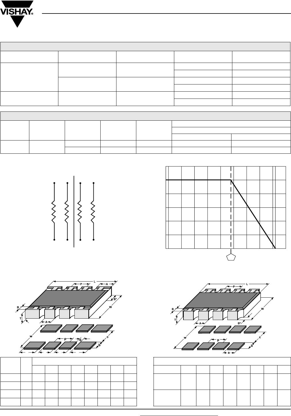
CRA06E, CRA06S
Vishay
Thick Film Resistor Array
Notes
(1)
Figures are given for a single element
(2)
Solderability is specified for 2 years after production or requalification. Permitted storage time is 20 years
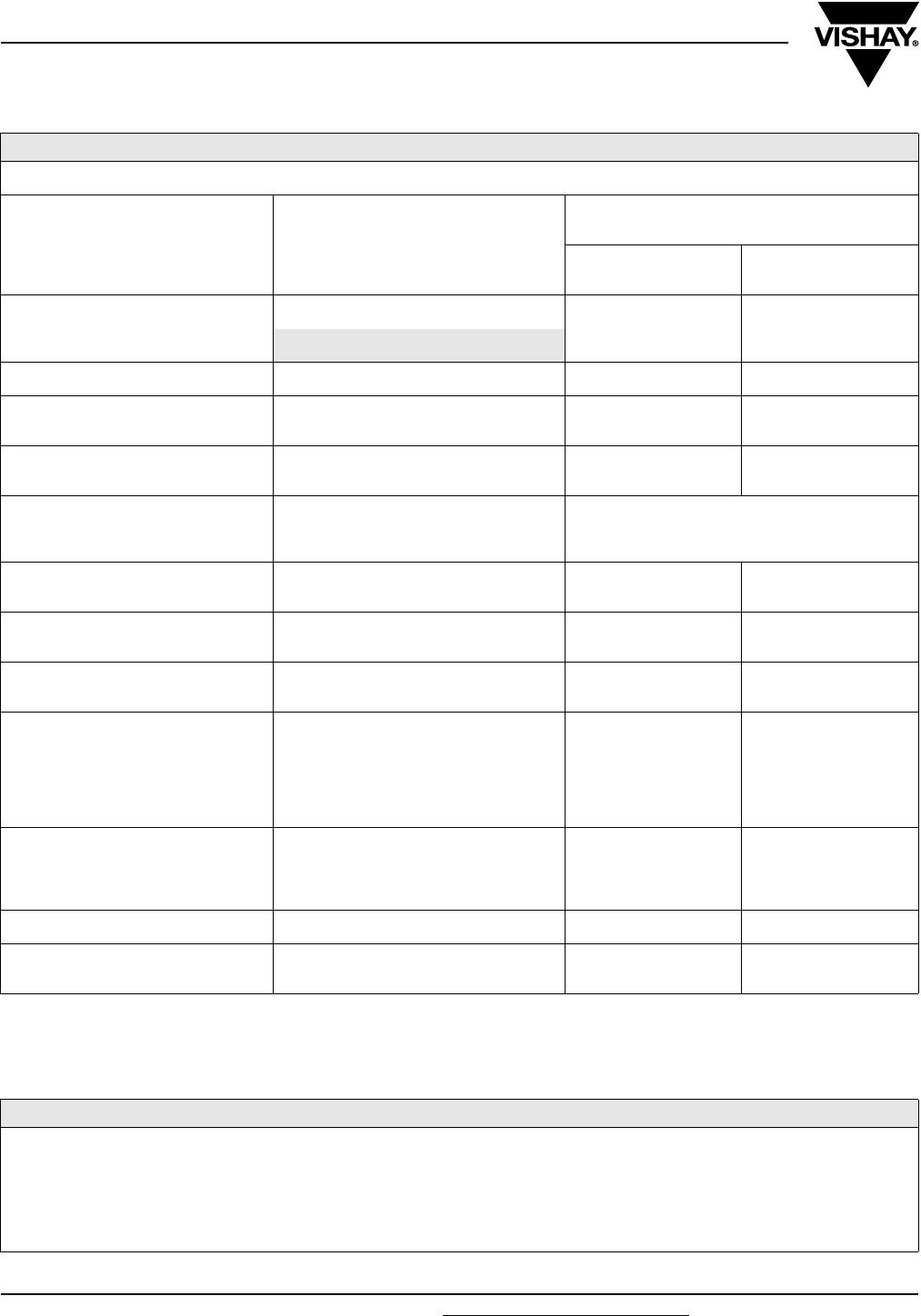
TEST PROCEDURES AND REQUIREMENTS
EN 60115-1
TEST
(clause)
CONDITIONS OF TEST
REQUIREMENTS
PERMISSIBLE CHANGE (ΔR/R)
(1)
STABILITY
CLASS 1 OR BETTER
STABILITY
CLASS 2 OR BETTER
Stability for product types:
10 Ω to 1 MΩ 10 Ω to 1 MΩ
CRA06E/CRA06S
Resistance (4.5) - ± 1 % ± 2 %; ± 5 %
Temperature coefficient (4.8.4.2)
20/- 55/20 °C and
20/125/20 °C
± 100 ppm/K ± 200 ppm/K
Overload (4.13)
U = 2.5 × (P
70
x R)
1/2
2 x U
max.
; 0.5 s
± (0.25 % R + 0.05 Ω) ± (0.5 % R + 0.05 Ω)
Solderability (4.17.5)
(2)
Aging 4 h at 155 °C, dryheat
solder bath method; 235 °C; 2 s
visual examination
Good tinning ( 95 % covered)
no visible damage
Resistance to soldering heat (4.18.2)
Solder bath method;
(260 ± 5) °C; (10 ± 1) s
± (0.25 % R + 0.05 Ω) ± (0.5 % R + 0.05 Ω)
Rapid change of temperature (4.19)
30 min at LCT = - 55 °C;
30 min at UCT = 125 °C; 5 cycles
± (0.25 % R + 0.05 Ω) ± (0.5 % R + 0.05 Ω)
Damp heat, steady state (4.24)
(40 ± 2) °C; 56 days;
(93 ± 3) % RH
± (1 % R + 0.05 Ω (2 % R + 0.1 Ω)
Climatic sequence (4.23)
16 h at UCT = 125 °C; 1 cycle at 55 °C;
2 h at LCT = - 55 °C;
1 h/1 kPa at 15 °C to 35 °C;
5 cycles at 55 °C
U = (P
70
x R)
1/2
U = U
max.
; whichever is less severe
± (1 % R + 0.05 Ω (2 % R + 0.1 Ω)
Endurance at 70 °C (4.25.1)
U = (P
70
x R)
1/2
U = U
max.
; whichever is less severe
1.5 h ON; 0.5 h OFF;
70 °C; 1000 h
± (1 % R + 0.05 Ω (2 % R + 0.1 Ω)
Extended endurance (4.25.1.8) Duration extended to 8000 h ± (2 % R + 0.1 Ω (4 % R + 0.1 Ω)
Endurance at upper category
temperature (4.25.3)
UCT = 125 °C; 1000 h ± (1 % R + 0.05 Ω (2 % R + 0.1 Ω)
APPLICABLE SPECIFICATIONS
EN 60115-1 Generic Specification
EN 140400 Sectional Specification
EN 140401-802 Detail Specification
IEC 60068-2-X Variety of environmental test procedures
EIA 481 Packaging of SMD components

CRA06S0431K47FTA

Mfr. #:
Manufacturer:
Vishay
Description:
Resistor Networks & Arrays CRA06S0403 1K47 1% RT1 e3
Lifecycle:
New from this manufacturer.
Delivery:
DHL FedEx Ups TNT EMS
Payment:
T/T Paypal Visa MoneyGram Western Union