• All specifi cations are subject to change without notice.
Features Applications
C Series
Mid Voltage (100 to 630V)
Type: C1005 [EIA CC0402], C1608 [EIA CC0603], C2012 [EIA CC0805],
C3216 [EIA CC1206], C3225 [EIA CC1210], C4532 [EIA CC1812], C5750 [EIA CC2220]
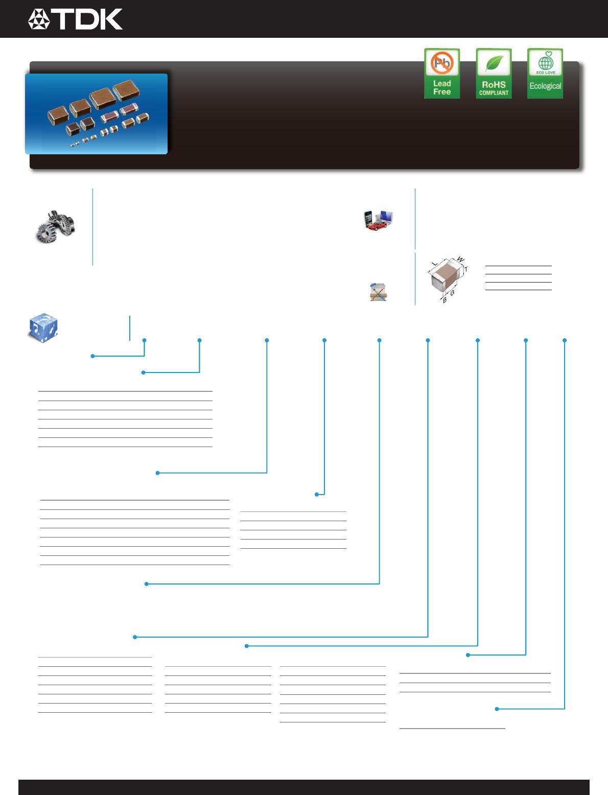
L Body Length
W Body Width
T Body Height
B Terminal Width
G Terminal Spacing
Shape &
Dimensions
Series Name
Dimensions L x W (mm)
Temperature Characteristics
Rated Voltage (DC)
Nominal Capacitance (pF)
Capacitance Tolerance
Packaging Style
Nominal Thickness
Code Length Width Terminal
C1005
1.00 ± 0.05 0.50 ± 0.05
0.10 min.
C1608
1.60 ± 0.10 0.80 ± 0.10
0.20 min.
C2012
2.00 ± 0.20 1.25 ± 0.20
0.20 min.
C3216
3.20 ± 0.20 1.60 ± 0.20
0.20 min.
C3225
3.20 ± 0.40 2.50 ± 0.30
0.20 min.
C4532
4.50 ± 0.40 3.20 ± 0.40
0.20 min.
C5750
5.70 ± 0.40 5.00 ± 0.40
0.20 min.
*Dimension tolerance are typical values
Code Tolerance
C
± 0.25pF
D
± 0.50pF
F±1%
G
±2%
J±5%
K
±10%
M ± 20%
Code Style
A 178 mm Reel, 4 mm Pitch
B 178 mm Reel, 2 mm Pitch
K 178 mm Reel, 8 mm Pitch
Temperature
Characteristics
Temperature
Range
CH
0±60 ppm/°C -25 to +85°C
C0G
0±30 ppm/°C -55 to +125°C
JB
±10% -25 to +85°C
X5R
±15% -55 to +85°C
X6S
±22% -55 to +105°C
X7R
±15% -55 to +125°C
X7S
±22% -55 to +125°C
X7T +22/-33%
-55 to +125°C
The capacitance is expressed in three digit codes and in units of pico Farads (pF).
The first and second digits identify the first and second significant figures of the
capacitance. The third digit identifies the multiplier. R designates a decimal point.
Ex. 0R2 = 0.2pF; 103 = 10,000pF; 105 = 1,000,000pF = 100nF
C • 3225 • X7R • 2A • 105 • K • 200 • A • A
Code Thickness
050 0.50 mm
060 0.60 mm
080 0.80 mm
085 0.85 mm
115 1.15 mm
125 1.25 mm
Special Reserved Code
Code Description
A, B, C TDK Internal Code
Code Voltage (DC)
2A 100V
2E 250V
2V 350V
2W 450V
2J 630V
Code Thickness
130 1.30 mm
160 1.60 mm
200 2.00 mm
230 2.30 mm
250 2.50 mm
280 2.80 mm
320 3.20 mm
• Snubber in power supply
• Electric flash circuits in digital still camera
• Power factor improvement
• Input-output filter in power supply
• Driver circuit in plasma display
• Noise bypass
• 9ROWDJHUDWLQJRI9WR9ZLWKFDSDFLWDQFHUDQJHXSWRȝ)
• High capacitance has been achieved through precision technologies
that enable the use of multiple thinner ceramic dielectric layers.
• Low residual inductance assures superior frequency characteristics.
• Excellent DC Bias properties.
• A lineup with wide-ranging rated voltages that enables selections that
are suitable for needs.
Catalog Number
Construction
Temperature Coefficient or
Capacitance Change
Page 2
MULTILAYER CERAMIC CHIP CAPACITORS
20150309 / mlcc_commercial_midvoltage_en