7
4688D–RFID–03/07
U3280M
4.3 Power Supply
The U3280M has a power management that handles two power supply sources. Normally, the
IC is supplied by a battery at the V
Batt
pin. If a magnetic field is applied at the LC-resonant circuit
of the device, the field detection circuit switches automatically from V
Batt
to field supply.
The V
DD
pin is used to connect a capacitor to smooth the voltage from the rectifier and to buffer
the power while the field is modulated by gaps and damping. The EEPROM and the connected
controller always operate with the voltage at the V
DD
pin.
Note: During field supply the maximum energy from the field is used if a high level is applied at the MOD
input.
4.3.1 Automatic Power Management
There are different conditions that cause a switch from the battery to field and back from field to
the battery.
The power management switches from battery to field if the rectified voltage (V
coil
) from the coil
inputs becomes higher than the field-on-detection voltage (V
FDon
), even if no battery voltage is
available (0 < V
Batt
< 1.8V). It switches back to battery if the coil voltage becomes lower than the
field-off-detection voltage (V
FDoff
).
The field detection stage of the power management has low pass characteristics to suppress
noise. An applied field needs a time delay t
BFS
(battery-to-field switch delay) to change the
power supply. If the field is removed from the coil, the power management will generate a reset
that can be connected to the microcontroller.
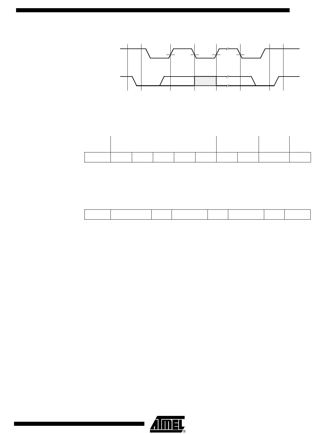
Figure 4-3. Switch Conditions for Power Management
Note: The rectified supply voltage from the coil is limited to V
DDC
(2.9V). During field supply, the battery
is switched off and V
DD
changes to V
DDC
.
4.3.2 Controlling Power Management via the Serial Interface
The automatic mode of the power management can be switched off and on by a command from
the microcontroller. If the automatic mode is switched off, the IC is always supplied by the bat-
tery up to the next power-on reset or to a switch-on command. The power management’s on and
off command must be transferred via the serial interface.
If the power management is switched off and the device is supplied from the battery, it can com-
municate via the field without loading the field. This mode can be used to realize applications
with battery supply if the field is too weak to supply the IC with power.
Battery
supply
Field
supply
V
Coil
> V
FDon
for t > t
BFS
V
Coil
< V
FDon
for t > t
BFS
(V
Batt
)
8
4688D–RFID–03/07
U3280M
4.3.3 Buffer Capacitor C
B
The buffer capacitor connected at V
DD
is used to buffer the supply voltage for the microcontroller
and the EEPROM during field supply. It smoothes the rectified AC from the coil and buffers the
supply voltage during modulation and gaps in the field. The size of this capacitor depends on the
application. It must be of a dimension so that during modulation and gaps the ripple on the sup-
ply voltage is in the range of 100 mV to 300 mV. During gaps and damping the capacitor is used
to supply the device, which means the size of the capacitor depends on the length of the gaps
and damping cycles.
4.4 Serial Interface
The transponder interface has a serial interface to the microcontroller for read and write access
to the EEPROM. In a special mode, the serial interface can also be used to control the
Bi-phase/Manchester modulator or the power management of the U3280M.
The serial interface of the U3280M device must be controlled by a master device (normally the
microcontroller) which generates the serial clock and controls the access via the SCL and SDA
lines. SCL is used to clock the data in and out of the device. SDA is a bi-directional line and used
to transfer data into and out of the device. The following protocol is used for the data transfers.
4.4.1 Serial Protocol
Data states on the SDA line change only when SCL is low.
Changes in the SDA line while SCL is high will be interpreted as a START or STOP condition.
A STOP condition is defined as a high-to-low transition on the SDA line while the SCL line is
high.
Each data transfer must be initialized with a START condition and terminated with a STOP
condition. The START condition awakens the device from standby mode, and the STOP
condition returns the device to standby mode.
A receiving device generates an acknowledge (A) after the reception of each byte. For that
purpose the master device must generate an extra clock pulse. If the reception was
successful, the receiving master or slave device pulls down the SDA line during that clock
cycle. If an acknowledge has not been detected (N) by the interface in transmit mode, it will
terminate further data transmissions and switch to receive mode. A master device must finish
its read operation by a not acknowledge and then issue a STOP condition to switch the
device to a known state.
Table 4-1. Example for a 350 µA Supply Current, 200 mV Ripple at V
DD
No Field Supply During Necessary C
B
250 µs 470 nF
500 µs 1000 nF
9
4688D–RFID–03/07
U3280M
Figure 4-4. Serial Protocol
Control Byte Format
The control byte follows the START condition and consists of the 5-bit row address, 2 mode con-
trol bits and the read/not-write bit.
After the STOP condition and before the START condition the device is in standby mode and
the SDA line is switched to an input with the pull-up resistor.
The START condition follows a control byte that determines the following operation. Bit 0 of
the control byte is used to control the following transfer direction. A “0” defines a write access
and a “1” defines a read access.
EEPROM address
Mode control
bits
Read/
NWrite
START A4 A3 A2 A1 A0 C1 C0 R/NW Ackn
Data Transfer Sequence
START Control byte Ackn Data byte Ackn Data byte Ackn STOP
START
condition
Data
valid
Data
change
Data/
acknowledge
valid
STOP
condition
SCL
SDA
Stand-
by
Stand-
by

U3280M-NFBY

Mfr. #:
Manufacturer:
Microchip Technology / Atmel
Description:
RFID Transponders RFID Interface IC 125kHz
Lifecycle:
New from this manufacturer.
Delivery:
DHL FedEx Ups TNT EMS
Payment:
T/T Paypal Visa MoneyGram Western Union

Products related to this Datasheet