BATTERY PROTECTION IC WITH CELL-BALANCE FUNCTION
S-8209B Series
Rev.3.3_00
Seiko Instruments Inc.
12
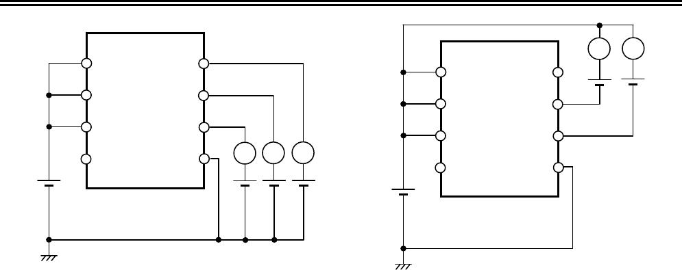
1. Normal status
In the S-8209B Series, both of CO and DO pin get the V
DD
level; the voltage between VDD and VSS (V
DS
) is more
than the overdischarge detection voltage (V
DL
), and is less than the overcharge detection voltage (V
CU
) and
respectively, the CTLC pin input voltage (V
CTLC
) > the CTLC pin voltage "L" (V
CTLCL
), the CTLD pin input voltage
(V
CTLD
) > the CTLD pin voltage "L" (V
CTLDL
). This is the normal status.
2. Overcharge status
In the S-8209B Series, the CO pin is in high impedance; when V
DS
gets V
CU
or more, or V
CTLC
gets V
CTLCL
or less.
This is the overcharge status.
If V
DS
gets the overcharge release voltage (V
CL
) or less, and V
CTLC
gets the CTLC pin voltage "H" (V
CTLCH
) or more,
the S-8209B Series releases the overcharge status to return to the normal status.
3. Overdischarge status
In the S-8209B Series, the DO pin is in high impedance; when V
DS
gets V
DL
or less, or V
CTLD
gets V
CTLDL
or less. This
is the overdischarge status.
If V
DS
gets the overdischarge release voltage (V
DU
) or more, and V
CTLD
gets the CTLD pin voltage "H" (V
CTLDH
) or
more, the S-8209B Series releases the overdischarge status to return to the normal status.
4. Cell-balance function
In the S-8209B Series, the CB pin gets the level of VDD pin; when V
DS
gets the cell-balance detection voltage (V
BU
)
or more. This is the charge cell-balance function.
If V
DS
gets the cell-balance release voltage (V
BL
) or less again, the S-8209B Series sets the CB pin the level of VSS
pin.
In addition, the CB pin gets the level of VDD pin; when V
DS
is more than V
DL
, and V
CTLD
is V
CTLDL
or less. This is the
discharge cell-balance function.
If V
CTLD
gets V
CTLDH
or more, or V
DS
is V
DL
or less again, the S-8209B Series sets the CB pin the level of VSS pin.
5. Delay circuit
In the S-8209B Series, users are able to set delay time which is from detection of changes in V
DS
, V
CTLC
, V
CTLD
to
output to the CO, DO, CB pin.
For example in the detection of overcharge status, when V
DS
exceeds V
CU
, or V
CTLC
gets V
CTLCH
or less, charging to
C
CDT
starts via R
CDT
. If the voltage between CDT and VSS (V
CDT
) reaches the CDT pin detection voltage (V
CDET
), the
CO pin is in high impedance. The output pin delay time t
D
is calculated by the following formula.
t
D
[s] = 10.0 M
Ω
(typ.) × C
CDT
[μF]
The electric charge in C
CDT
starts to be discharged when the delay time has finished.
The delay time that users have set for the CO pin, as seen above, is settable for each output pin DO, CB.