MSMP17A-M3/89A

MSMP6.0A thru MSMP20A
www.vishay.com
Vishay General Semiconductor
Revision: 10-Dec-13
1
Document Number: 89457
For technical questions within your region: DiodesAmericas@vishay.com
, DiodesAsia@vishay.com, DiodesEurope@vishay.com
THIS DOCUMENT IS SUBJECT TO CHANGE WITHOUT NOTICE. THE PRODUCTS DESCRIBED HEREIN AND THIS DOCUMENT
ARE SUBJECT TO SPECIFIC DISCLAIMERS, SET FORTH AT www.vishay.com/doc?91000
Surface Mount TRANSZORB
®
Transient Voltage Suppressors
TYPICAL APPLICATIONS
Use in sensitive electronics protection against voltage
transients induced by inductive load switching and lighting
on ICs, MOSFET, signal lines of sensor units for protecting
sensitive equipment against transient overvoltages.
FEATURES
Very low profile - typical height of 0.65 mm
Ideal for automated placement
Oxide planar chip junction
Uni-directional polarity only
Peak pulse power: 150 W (10/1000 μs)
ESD capability: 15 kV (air), 8 kV (contact)
Meets MSL level 1, per J-STD-020C, LF maximum peak of
260 °C
Material categorization: For definitions of compliance
please see www.vishay.com/doc?99912
MECHANICAL DATA
Case: MicroSMP
Molding compound meets UL 94 V-0 flammability rating
Base P/N-M3 - halogen-free, RoHS-compliant, and
commercial grade
Terminals: Matte tin plated leads, solderable per
J-STD-002 and JESD 22-B102
M3 suffix meets JESD 201 class 2 whisker test
Polarity: Color band denotes the cathode end
Notes
(1)
Non-repetitive current pulse, per fig. 1
(2)
Mounted on 6.0 mm x 6.0 mm copper pads to each terminal
(3)
Mounted on minimum recommended pad layout
PRIMARY CHARACTERISTICS
V
BR
6.67 V to 24.5 V
V
WM
6.0 V to 20 V
P
PPM
(10 x 1000 μs) 150 W
T
J
max. 150 °C
Polarity Uni-directional
Package MicroSMP
MicroSMP
eSMP
®
Series
Top View
Bottom View
MAXIMUM RATINGS (T
A
= 25 °C unless otherwise noted)
PARAMETER SYMBOL VALUE UNIT
Peak power dissipation with a 10/1000 μs waveform (fig. 1) P
PPM
(1)(2)
150 W
Peak pulse current with a 10/1000 μs waveform I
PPM
(1)
See next table A
Power dissipation T
M
= 120 °C P
D
(2)
1.0
W
Power dissipation T
A
= 25 °C P
D
(3)
0.5
Operating junction and storage temperature range T
J
, T
STG
- 55 to + 150 °C
MSMP6.0A thru MSMP20A
www.vishay.com
Vishay General Semiconductor
Revision: 10-Dec-13
2
Document Number: 89457
For technical questions within your region: DiodesAmericas@vishay.com
, DiodesAsia@vishay.com, DiodesEurope@vishay.com
THIS DOCUMENT IS SUBJECT TO CHANGE WITHOUT NOTICE. THE PRODUCTS DESCRIBED HEREIN AND THIS DOCUMENT
ARE SUBJECT TO SPECIFIC DISCLAIMERS, SET FORTH AT www.vishay.com/doc?91000
Notes
(1)
Pulse test: t
p
50 ms
(2)
Surge current waveform per Fig. 1 and derate per Fig. 3
(3)
To calculate maximum clamping voltage at surge current uses the following formula: V
CL max.
= R
D
x I
PP
+ V
BR max.
Notes
(1)
Free air, mounted on recommended PCB 1 oz. pad area; thermal resistance R
JA
- junction to ambient
(2)
Units mounted on PCB with 6.0 mm x 6.0 mm copper pad areas; R
JM
- junction to mount
Notes
(1)
Immunity to IEC 61000-4-2 air discharge mode has a typical performance > 30 kV
(2)
System ESD standard
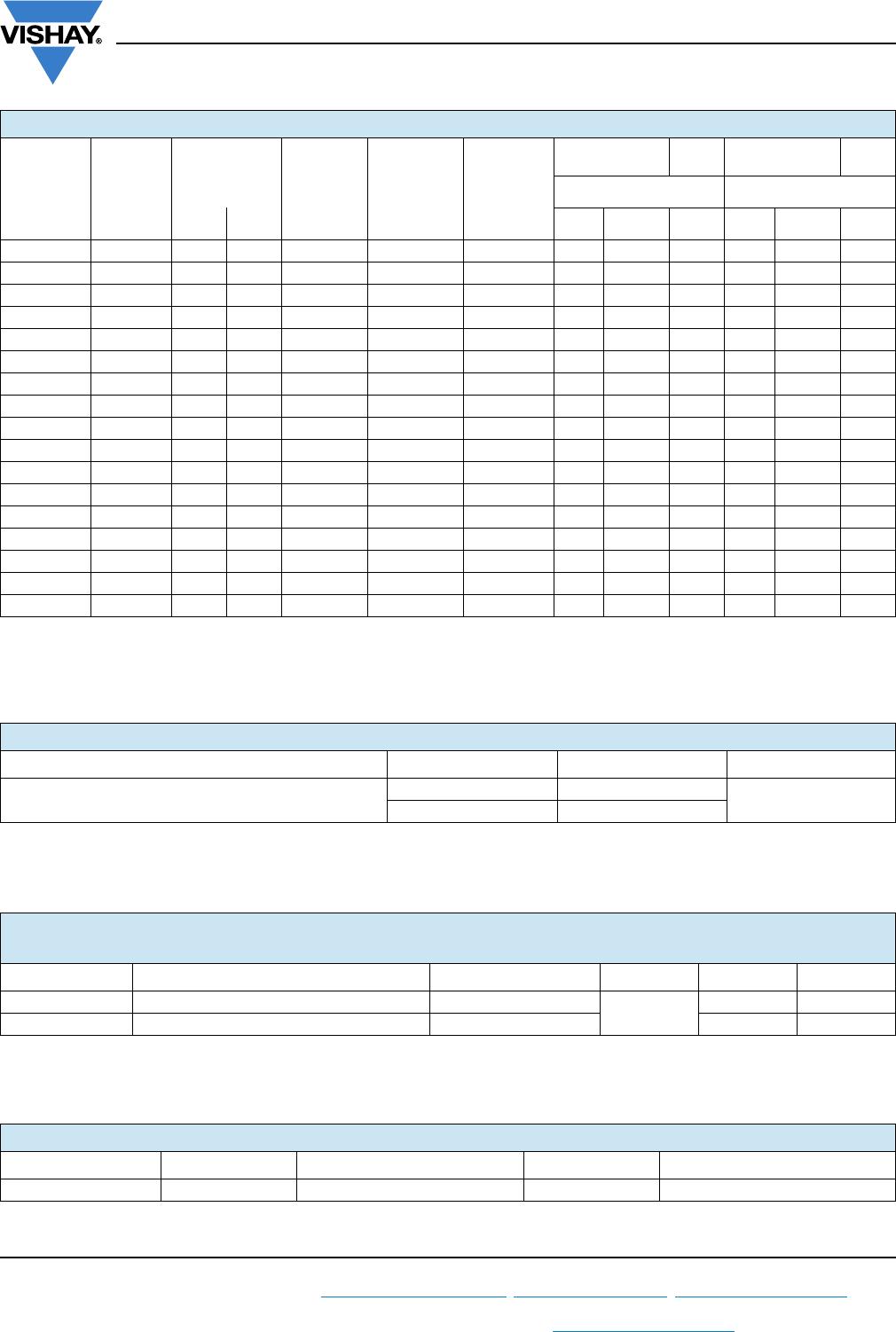
ELECTRICAL CHARACTERISTICS (T
A
= 25 °C unless otherwise noted)
DEVICE
TYPE
DEVICE
MARKING
CODE
BREAKDOWN
VOLTAGE
V
BR
AT I
T
(1)
(V)
TEST
CURRENT
I
T
(mA)
STAND-OFF
VOLTAGE
V
WM
(V)
MAXIMUM
REVERSE
LEAKAGE
CURRENT
I
R
AT V
WM
(μA)
MAXIMUM
V
C
AT I
PPM
R
D
MAXIMUM
V
C
AT I
PPM
R
D
10/1000 μs 8/20 μs
MIN. MAX. V
C
(V) I
PPM
(A) R
D
()V
C
(V) I
PPM
(A) R
D
()
MSMP6.0A AG 6.67 7.37 10 6.0 200 10.3 14.6 0.201 13.7 73.0 0.087
MSMP6.5A AK 7.22 7.98 10 6.5 100 11.2 13.4 0.240 14.5 69.0 0.095
MSMP7.0A AM 7.78 8.60 10 7.0 50 12.0 12.5 0.272 15.7 63.7 0.111
MSMP7.5A AP 8.33 9.21 1.0 7.5 50 12.9 11.6 0.317 17.0 58.8 0.132
MSMP8.0A AR 8.89 9.83 1.0 8.0 20 13.6 11.0 0.342 18.2 54.9 0.152
MSMP8.5A AT 9.44 10.4 1.0 8.5 2.0 14.4 10.4 0.384 19.5 51.3 0.177
MSMP9.0A AV 10.0 11.1 1.0 9.0 2.0 15.4 9.7 0.441 20.6 48.6 0.195
MSMP10A AX 11.1 12.3 1.0 10 1.0 17.0 8.8 0.533 21.7 46.1 0.204
MSMP11A AZ 12.2 13.5 1.0 11 1.0 18.2 8.2 0.570 24.4 41.0 0.266
MSMP12A BE 13.3 14.7 1.0 12 1.0 19.9 7.5 0.690 25.3 39.5 0.268
MSMP13A BG 14.4 15.9 1.0 13 1.0 21.5 7.0 0.803 27.2 36.8 0.307
MSMP14A BK 15.6 17.2 1.0 14 1.0 23.2 6.5 0.928 29.5 33.9 0.364
MSMP15A BM 16.7 18.5 1.0 15 1.0 24.4 6.2 0.960 32.5 30.8 0.455
MSMP16A BP 17.8 19.7 1.0 16 1.0 26.0 5.8 1.092 34.7 28.8 0.520
MSMP17A BR 18.9 20.9 1.0 17 1.0 27.6 5.4 1.233 36.8 27.2 0.586
MSMP18A BT 20.0 22.1 1.0 18 1.0 29.2 5.1 1.382 39.3 25.4 0.676
MSMP20A BV 22.2 24.5 1.0 20 1.0 32.4 4.6 1.706 42.8 23.4 0.783
THERMAL CHARACTERISTICS (T
A
= 25 °C unless otherwise noted)
PARAMETER SYMBOL VALUE UNIT
Typical thermal resistance
R
JA
(1)
250
°C/W
R
JM
(2)
30
IMMUNITY TO STATIC ELECTRICAL DISCHARGE TO THE FOLLOWING STANDARDS
(T
A
= 25 °C unless otherwise noted)
STANDARD TEST TYPE TEST CONDITIONS SYMBOL CLASS VALUE
AEC-Q101-001 Human body model (contact mode) C = 100 pF, R = 1.5 k
V
C
H3B > 8 kV
IEC 61000-4-2
(2)
Human body model (air discharge mode)
(1)
C = 150 pF, R = 330 4 > 15 kV
ORDERING INFORMATION (Example)
PREFERRED P/N UNIT WEIGHT (g) PREFERRED PACKAGE CODE BASE QUANTITY DELIVERY MODE
MSMP6.0A-M3/89A 0.006 89A 4500 7" diameter plastic tape and reel
MSMP6.0A thru MSMP20A
www.vishay.com
Vishay General Semiconductor
Revision: 10-Dec-13
3
Document Number: 89457
For technical questions within your region: DiodesAmericas@vishay.com
, DiodesAsia@vishay.com, DiodesEurope@vishay.com
THIS DOCUMENT IS SUBJECT TO CHANGE WITHOUT NOTICE. THE PRODUCTS DESCRIBED HEREIN AND THIS DOCUMENT
ARE SUBJECT TO SPECIFIC DISCLAIMERS, SET FORTH AT www.vishay.com/doc?91000
RATINGS AND CHARACTERISTICS CURVES
(T
A
= 25 °C unless otherwise noted)
Fig. 1 - Pulse Waveform
Fig. 2 - Peak Pulse Power Rating Curve
Fig. 3 - Pulse Power or Current vs. Initial Junction Temperature
Fig. 4 - Typical Junction Capacitance
Fig. 5 - Power Dissipation Derating Curve
Fig. 6 - Typical Transient Thermal Impedance
0
0
50
100
150
1.0 2.0 3.0 4.0
t
r
= 10 μs
t
r
= 8 μs
t
d
= 1000 μs
t
d
= 20 μs
I
PPM
- Peak Pulse Current (% I
RSM
)
t - Time (ms)
t
d
Peak Value
I
PPM
Half Value -
I
PPM
I
PP
2
T
J
= 25 °C
Pulse Width (t
d
) is
Dened as the Point
Where the Peak Current
Decays to 50 % of I
PPM
0.1
0.01
0.1
1
10
100
1 10 100 1000 10 000
P
PPM
- Peak Pulse Power (kW)
t
d
- Pulse Width (μs)
0.24" x 0.24" (6.0 mm x 6.0 mm)
Copper Pad Areas
Non-Repetitive Pulse
Waveform Shown in Fig. 1
T
A
= 25 °C
50
75
100
25
0
0 50 75 100 125 175
Peak Pulse Power (P
PP
) or Current (I
PP
)
Derating in Percentage (%)
T
J
- Initial Temperature (°C)
25 150
10
100
1000
6 8 10 12 14 16 18 20
C
J
- Junction Capacitance (pF)
V
WM
- Reverse Stand-Off Voltage (V)
Measured at Stand-off
Voltage, V
WM
Measured at Zero Bias
T
J
= 25 °C
f = 1.0 MHz
V
sig
= 50 mV
p-p
0.0
0.2
0.4
0.6
0.8
1.0
1.2
500 100 150 175
Ambient Temperature (°C)
P
D
- Power Dissipation (W)
25 75 125
Mounted on Minimum
Recommende Pad Area
T
A
= T
M
, Mounted on
6.0 mm x 6.0 mm Copper Pad
1000
100
10
0.10.01 1 10 100 1000
t - Pulse Duration (s)
Transient Thermal Impedance (°C/W)
Junction to Ambient

MSMP17A-M3/89A

Mfr. #:
Manufacturer:
Vishay Semiconductors
Description:
TVS Diodes / ESD Suppressors 150W,17V UNIDIR,Micro-SMP TVS
Lifecycle:
New from this manufacturer.
Delivery:
DHL FedEx Ups TNT EMS
Payment:
T/T Paypal Visa MoneyGram Western Union