MAX3747BEUB+

Detailed Description
The limiting amplifiers consist of a multistage amplifier,
offset-correction circuitry, an output buffer, and loss-of-
signal detect circuitry (see the
Functional Diagram
).
Input Stage
The input stage is shown in Figure 3. It provides 50 ter-
mination to V
REF
for each input signal, IN+ and IN-. The
MAX3747A/MAX3747B should be AC-coupled.
Multistage Amplifier
The high-bandwidth multistage amplifier provides approx-
imately 61dB of gain for the MAX3747A/MAX3747B.
Offset Correction Loop
The MAX3747A/MAX3747B are susceptible to DC offsets
in the signal path because they have high gain. In com-
munication systems using NRZ data with a 50% duty
cycle, pulse-width distortion present in the signal or gener-
ated in the transimpedance amplifier appears as an input
offset and is reduced by the offset correction loop.
The offset correction loop sets a low-frequency cutoff of
3.2kHz.
MAX3747A/MAX3747B
155Mbps to 3.2Gbps, Low-Power SFP
Limiting Amplifiers
7
Maxim Integrated
Pin Description
NAME
PIN
MAX3747A/
MAX3747B
MICREL
SY8893V
FUNCTION
1 DISABLE EN
Disable Function Pin. The data outputs are held static when this pin is asserted high,
transistor-to-transistor logic (TTL). The data outputs are enabled when this pin is held
low. LOS functions remain active when outputs are disabled. For normal operation
connect to GND.
2 IN+ DIN Noninverted Input Signal
3
IN-
DIN Inverted Input Signal
4V
REF
V
REF
Reference Voltage for LOS Threshold Setting
5 TH LOSLVL
Loss-of-Signal Level Set. A voltage on this pin created by a two-resistor divider sets
the threshold level. Connect one resistor from this pin to V
CC
and another from this pin
to V
REF
(see Figure 5).
6 GND GND Ground
7 LOS LOS
Loss of Signal. Open collector for the MAX3747A; internal 100kpullup to V
CC
for the
MAX3747B. LOS is high when the level of the input signal drops below the preset
threshold set by the TH input. LOS is deasserted low when the signal level is above
the threshold.
8
OUT-
DOUT Inverted Data Output, CML
9 OUT+ DOUT Noninverted Data Output, CML
10 V
CC
V
CC
Positive Power Supply
MAX3747A
MAX3747B
50
50
V
REF
V
CC
ESD
STRUCTURES
Figure 3. Differential Input Stage
MAX3747A/MAX3747B
155Mbps to 3.2Gbps, Low-Power SFP
Limiting Amplifiers
8
Maxim Integrated
CML Output Buffer
The CML outputs of the MAX3747A/MAX3747B limiting
amplifiers provide high tolerance to impedance mis-
matches and inductive connectors. The output current
is approximately 16mA for the MAX3747A/MAX3747B.
Connecting the DISABLE pin to V
CC
disables the out-
put. If the LOS pin is connected to the DISABLE pin,
the outputs OUT+ and OUT- are at a static voltage
(squelch) whenever the input signal level drops below
the LOS threshold. The output buffer can be AC- or DC-
coupled to the load (Figure 4).
The MAX3747A/MAX3747B output is 800mV
P-P
.
MAX3747A
MAX3747B
50
50
DIGITAL
OFFSET
CORRECTION
V
REF
SIGNAL DETECT
50
50
IN+
IN-
V
REF
V
REF
TH LOS
V
CC
V
CC
OUT+
DISABLE
OUT-
R
TH1
R
TH1
+ R
TH2
5k
R
TH2
Functional Diagram
50
50
V
CC
OUT+
OUT-
DISABLEDISABLE
Q4 Q2Q1Q3
DISABLE
DATA
ESD
STRUCTURES
Figure 4. CML Output Buffer
MAX3747A/MAX3747B
155Mbps to 3.2Gbps, Low-Power SFP
Limiting Amplifiers
9
Maxim Integrated
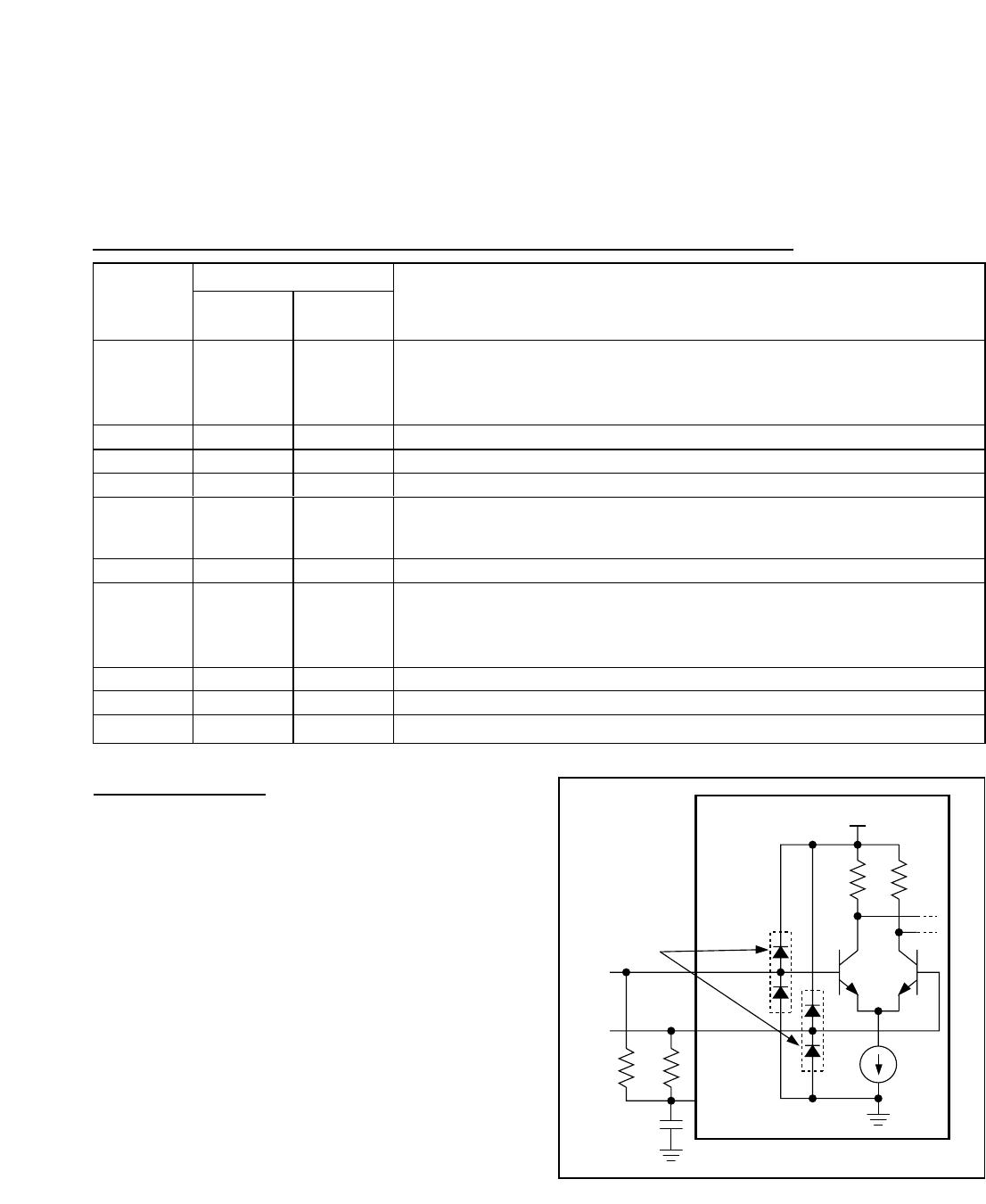
Loss-of-Signal Indicator
The MAX3747A/MAX3747B are equipped with LOS cir-
cuitry that indicates when the input signal is below a pro-
grammable threshold, set by a voltage on the TH pin
(see the
Typical Operating Characteristics
). The voltage
on the TH pin is set by two resistors, one connecting
from the TH pin to V
CC
and the other connecting from TH
to V
REF
(Figure 5). An RMS power detector compares
the input signal amplitude with this threshold and feeds
the signal-detect information to the LOS output, which is
open collector. To prevent LOS chatter in the region of
the programmed threshold, approximately 2dB of hys-
teresis is built into the LOS assert/deassert function.
Once asserted, LOS is not deasserted until the input
amplitude rises to the required level. Figure 6 shows the
LOS output circuit.
Applications Information
Program the LOS Assert Threshold
Program the LOS assert threshold according to Figure
5. The combination of R
TH1
and R
TH2
should be
greater than or equal to 5k, see the Assert/Deassert
vs. V
TH
graph in the
Typical Operating Characteristics
.
Select the Coupling Capacitor
When AC-coupling is desired, coupling capacitors C
IN
and C
OUT
should be selected to minimize the receiv-
er’s deterministic jitter. Jitter is decreased as the input
low-frequency cutoff (f
IN
) is decreased:
f
IN
= 1/[2π(50)(C
IN
)]
For all applications, the recommended value for C
IN
and C
OUT
is 0.1µF, which provides f
IN
equal to 32kHz.
Refer to Application Note HFAN-1.1:
Choosing AC-
Coupling Capacitors
on the Maxim website
(www.maximintegrated.com)
.
TH
V
REF
R
TH1
R
TH2
V
CC
V
TH
= (R
TH2
x (V
REF
- V
CC
)) / (R
TH1
+ R
TH2
)
V
TH
IS V
CC
REFERENCED
R
TH1
+ R
TH2
5k
Figure 5. MAX3747A/MAX3747B LOS Threshold Circuit
ESD
STRUCTURE
V
CC
LOS
*
*100kPULLUP (MAX3747B ONLY)
Figure 6. MAX3747A/MAX3747B LOS Output Circuit

MAX3747BEUB+

Mfr. #:
Manufacturer:
Maxim Integrated
Description:
Limiting Amplifiers 155-3.2Gbps SFP
Lifecycle:
New from this manufacturer.
Delivery:
DHL FedEx Ups TNT EMS
Payment:
T/T Paypal Visa MoneyGram Western Union