©2013 Integrated Device Technology, Inc.
1
OCTOBER 2013
DSC-5622/7
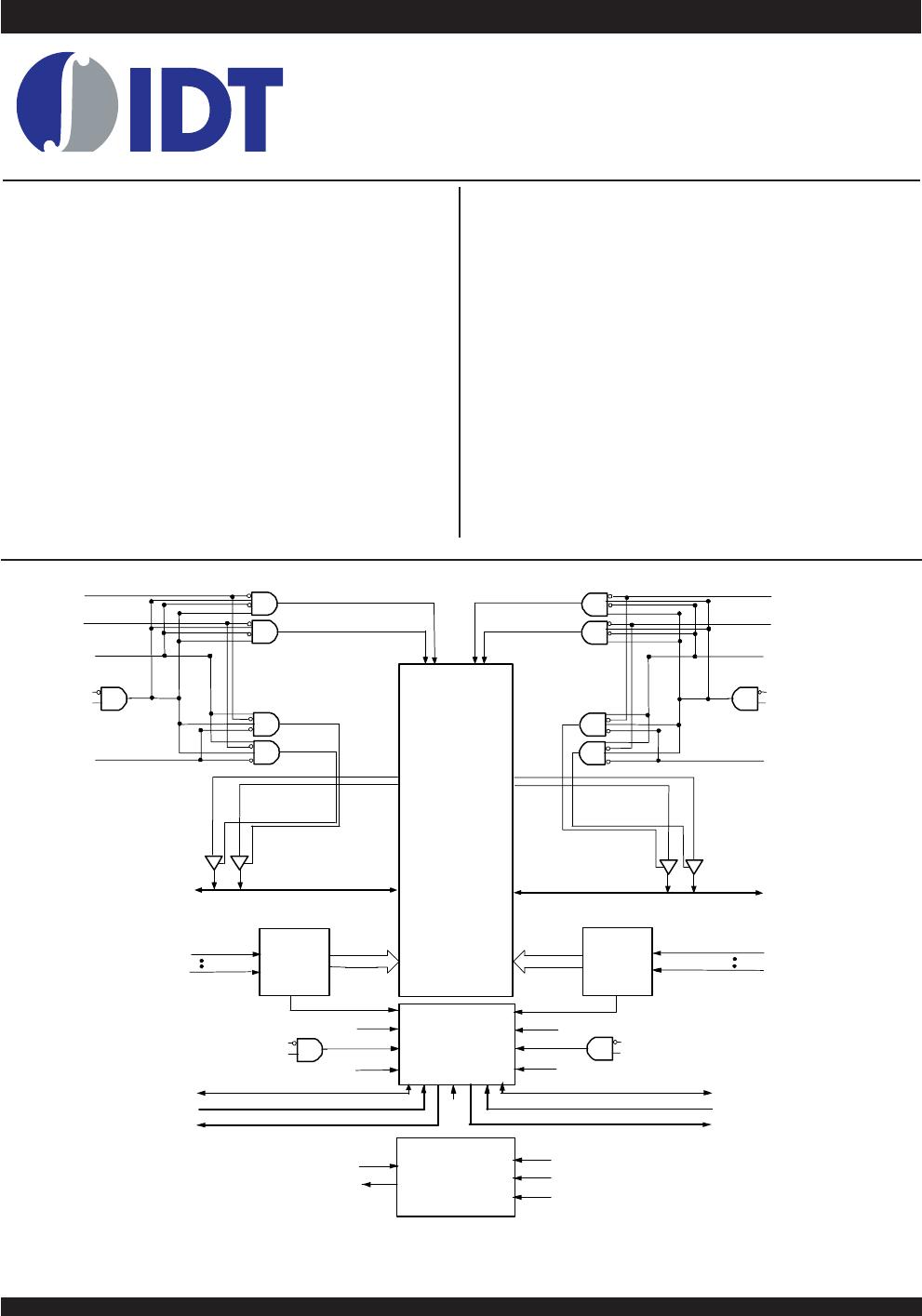
Functional Block Diagram
Fully asynchronous operation from either port
Separate byte controls for multiplexed bus and bus
matching compatibility
Supports JTAG features compliant to IEEE 1149.1
Due to limited pin count, JTAG is not supported on the
128-pin TQFP package.
LVTTL-compatible, single 3.3V (±150mV) power supply for
core
LVTTL-compatible, selectable 3.3V (±150mV)/2.5V (±100mV)
power supply for I/Os and control signals on each port
Available in a 128-pin Thin Quad Flatpack, 208-ball fine
pitch Ball Grid Array, and 256-ball Ball Grid Array
Industrial temperature range (–40°C to +85°C) is available
for selected speeds
Green parts available, see ordering information
Features
True Dual-Port memory cells which allow simultaneous
access of the same memory location
High-speed access
Commercial: 10/12/15ns (max.)
Industrial: 12ns (max.)
Dual chip enables allow for depth expansion without
external logic
IDT70V631 easily expands data bus width to 36 bits or
more using the Master/Slave select when cascading more
than one device
M/S = VIH for BUSY output flag on Master,
M/S = VIL for BUSY input on Slave
Busy and Interrupt Flags
On-chip port arbitration logic
Full on-chip hardware support of semaphore signaling
between ports
HIGH-SPEED 3.3V 256K x 18
ASYNCHRONOUS DUAL-PORT
STATIC RAM
IDT70V631S
NOTES:
1. BUSY is an input as a Slave (M/S=V
IL) and an output when it is a Master (M/S=VIH).
2. BUSY and INT are non-tri-state totem-pole outputs (push-pull).
CE
0R
R/
W
R
CE
1R
LB
R
UB
R
256K x 18
MEMORY
ARRAY
Address
Decoder
A
17R
A
0R
Address
Decoder
CE
0L
R/
W
L
CE
1L
LB
L
UB
L
Dout0-8_L
Dout9-17_L
Dout0-8_R
Dout9-17_R
B
E
0
L
B
E
1
L
B
E
1
R
B
E
0
R
I/O
0L
- I/O
17L
I/O
0R
-I/O
17R
Din_L
ADDR_L
Din_R
ADDR_R
OE
R
OE
L
ARBITRATION
INTERRUPT
SEMAPHORE
LOGIC
SEM
L
INT
L
BUSY
L
M/S
R/W
L
OE
L
R/W
R
OE
R
BUSY
R
SEM
R
INT
R
CE
0L
CE
1L
CE
0R
CE
1R
TMS
TCK
TRST
TDI
TDO
JTAG
5622 drw 01
A
17L
A
0L
IDT70V631S
High-Speed 3.3V 256K x 18 Asynchronous Dual-Port Static RAM Industrial and Commercial Temperature Ranges
2
Description
The IDT70V631 is a high-speed 256K x 18 Asynchronous Dual-Port
Static RAM. The IDT70V631 is designed to be used as a stand-alone
4608K-bit Dual-Port RAM or as a combination MASTER/SLAVE Dual-
Port RAM for 36-bit-or-more word system. Using the IDT MASTER/
SLAVE Dual-Port RAM approach in 36-bit or wider memory system
applications results in full-speed, error-free operation without the need for
additional discrete logic.
This device provides two independent ports with separate control,
address, and I/O pins that permit independent, asynchronous access for
reads or writes to any location in memory. An automatic power down
feature controlled by the chip enables (either CE
0 or CE1) permit the
on-chip circuitry of each port to enter a very low standby power mode.
The 70V631 can support an operating voltage of either 3.3V or 2.5V
on one or both ports, controlled by the OPT pins. The power supply for
the core of the device (VDD) remains at 3.3V.
Pin Configurations
(1,2,3,4)
NOTES:
1. All V
DD pins must be connected to 3.3V power supply.
2. All V
DDQ pins must be connected to appropriate power supply: 3.3V if OPT pin for that port is set to VIH (3.3V) and 2.5V if OPT pin for that port is
set to V
IL (0V).
3. All V
SS pins must be connected to ground.
4. Package body is approximately 15mm x 15mm x 1.4mm with 0.8mm ball pitch.
5. This package code is used to reference the package diagram.
6. This text does not indicate orientation of the actual part-marking.
1716
15
1412 13
10
9876543
21
11
A
B
C
D
E
F
G
H
J
K
L
M
N
P
R
T
U
I/O
9L
NC V
SS
A
4L
INT
L
SEM
L
NCA
8L
A
12L
A
16L
V
SS
NCOPT
L
A
0L
NC V
SS
NC
NC
A
1L
A
5L
BUSY
L
V
SS
CE
0L
CE
1L
NC
A
9L
A
13L
A
17L
I/O
8L
V
DDQR
V
SS
V
DD Q L
I/O
9R
V
DD Q R
V
DD
A
2L
A
6
L
R/
W
L
V
SS
UB
L
A
10L
A
14L
NC
NC
I/O
8R
V
DD
I/O
11L
V
SS
I/O
10L
NC V
DD
A
3L
NC
OE
L
NC
I/O
11R
V
DDQR
I/O
10R
V
DD Q L
NC
NC
V
SS
NC
V
SS
I/O
12L
NC
V
DD
NC
V
DDQR
I/O
12R
V
DDQL
V
DD
V
SS
V
SS
NC I/O
14L
V
DDQR
V
DD Q L
NC
I/O
15R
V
SS
I/O
7R
V
DDQL
I/O
7L
A
15L
A
11L
A
7L
LB
L
I/O
6L
NC V
SS
NC
V
SS
I/O
6R
NC
NC V
DDQL
I/O
5L
NC
V
DD
NC
V
SS
I/O
5R
V
SS
V
DDQR
I/O
3R
V
DDQL
I/O
4R
V
SS
I/O
4L
V
SS
I/O
3L
NC
A
0R
A
1R
A
2R
A
3R
A
4R
A
5R
A
6R
I/O
1R
NC
V
SS
NC I/O
15L
A
16R
A
12R
A
8R
NC
V
DD
SEM
R
INT
R
V
DDQR
NC I/O
1L
NC
V
SS
NC I/O
17R
A
17R
A
13R
A
9R
NC
CE
0R
CE
1R
V
DD
V
SS
BUSY
R
V
SS
V
DD
V
SS
V
DDQL
I/O
0R
V
DDQR
NC I/O
17L
V
DDQL
NC
NC
A
14R
A
10R
UB
R
V
SS
NC
NC
V
SS
I/O
2R
NC
V
SS
NC
V
DD
A
15R
A
11R
A
7R
LB
R
OE
R
M/
S
R/
W
R
V
DDQL
I/O
2L
OPT
R
NC I/O
0L
70V631BF
BF-208
(5)
208-Ball BGA
Top View
(6)
5622 tbl 02b
I/O
13L
I/O
14R
V
SS
I/O
13R
V
SS
I/O
16R
I/O
16 L
V
DDQR
NC
A
B
C
D
E
F
G
H
J
K
L
M
N
P
R
T
U
V
SS
NC
NC
V
DDQR
V
SS
V
DD
V
SS
NC
V
DD
V
DD
TDO
TDI
TCK
TMS
TRST
V
SS
09/30/03
3
IDT70V631S
High-Speed 3.3V 256K x 18 Asynchronous Dual-Port Static RAM Industrial and Commercial Temperature Ranges
NOTES:
1. All V
DD pins must be connected to 3.3V power supply.
2. All V
DDQ pins must be connected to appropriate power supply: 3.3V if OPT pin for that port is set to VIH (3.3V) and 2.5V if OPT pin for that port is
set to V
IL (0V).
3. All V
SS pins must be connected to ground.
4. Package body is approximately 14mm x 20mm x 1.4mm.
5. This package code is used to reference the package diagram.
6. This text does not indicate orientation of the actual part-marking.
7. Due to the restricted number of pins, JTAG is not supported in the PK-128 package.
1
2
3
4
5
6
7
8
9
10
11
12
13
14
15
16
17
18
19
20
21
22
23
24
25
26
27
28
29
30
31
32
33
34
35
36
37
38
102
101
100
99
98
97
96
95
94
93
92
90
89
88
87
86
85
84
83
82
81
80
79
78
77
76
75
74
73
72
70
69
68
67
66
65
91
71
A
14L
A
15L
A
16L
A
17L
IO
9L
IO
9R
V
DDQL
V
SS
IO
10L
IO
10R
V
DDQR
V
SS
IO
11L
IO
11R
IO
12L
IO
12R
V
DD
V
DD
V
SS
V
SS
IO
13R
IO
13L
IO
14R
IO
14L
IO
15R
IO
15L
V
DDQL
V
SS
IO
16R
IO
16L
V
DDQR
V
SS
IO
17R
IO
17L
A
17R
A
16R
A
15R
A
14R
A
1R
A
0R
OPT
R
IO
0L
IO
0R
V
DDQR
V
SS
IO
1L
IO
1R
V
DDQL
V
SS
IO
2L
IO
2R
IO
3L
IO
3R
IO
4L
IO
4R
V
SS
V
SS
V
DD
V
DD
IO
5L
IO
5R
V
DDQR
V
SS
IO
7R
IO
7L
V
DDQL
V
SS
NC
IO
8R
IO
8L
V
SS
OPT
L
A
0L
A
1L
IO
6R
IO
6L
70V631PRF
PK-128
(5)
128-Pin TQFP
Top View
(6)
5622 drw 02a
A
1
3
L
A
1
2
L
A
1
1
L
A
1
0
L
A
9
L
A
8
L
A
7
L
U
B
L
L
B
L
C
E
1
L
C
E
0
L
V
D
D
V
D
D
V
S
S
V
S
S
S
E
M
L
O
E
L
R
/
W
L
B
U
S
Y
L
I
N
T
L
N
C
A
6
L
A
5
L
A
4
L
A
3
L
A
2
L
A
1
3
R
A
1
2
R
A
1
1
R
A
1
0
R
A
9
R
A
8
R
A
7
R
U
B
R
L
B
R
C
E
1
R
C
E
0
R
V
D
D
V
D
D
V
S
S
V
S
S
S
E
M
R
O
E
R
R
/
W
R
B
U
S
Y
R
I
N
T
R
M
/
S
A
6
R
A
5
R
A
4
R
A
3
R
A
2
R
3
9
4
0
4
1
4
2
4
3
4
4
4
5
4
6
4
7
4
8
4
9
5
0
5
1
5
2
5
3
5
4
5
5
5
6
5
7
5
8
5
9
6
0
6
1
6
2
6
3
6
4
1
2
8
1
2
7
1
2
6
1
2
5
1
2
4
1
2
3
1
2
2
1
2
1
1
2
0
1
1
9
1
1
8
1
1
7
1
1
6
1
1
5
1
1
4
1
1
3
1
1
2
1
1
1
1
1
0
1
0
9
1
0
8
1
0
7
1
0
6
1
0
5
1
0
4
1
0
3
.
09/30/03
Pin Configurations
(1,2,3,4,7)
(con't.)

70V631S12BCI8

Mfr. #:
Manufacturer:
IDT
Description:
SRAM 256Kx18 STD-PWR 3.3V DUAL-PORT RAM
Lifecycle:
New from this manufacturer.
Delivery:
DHL FedEx Ups TNT EMS
Payment:
T/T Paypal Visa MoneyGram Western Union