IDT70V631S
High-Speed 3.3V 256K x 18 Asynchronous Dual-Port Static RAM Industrial and Commercial Temperature Ranges
14
NOTES:
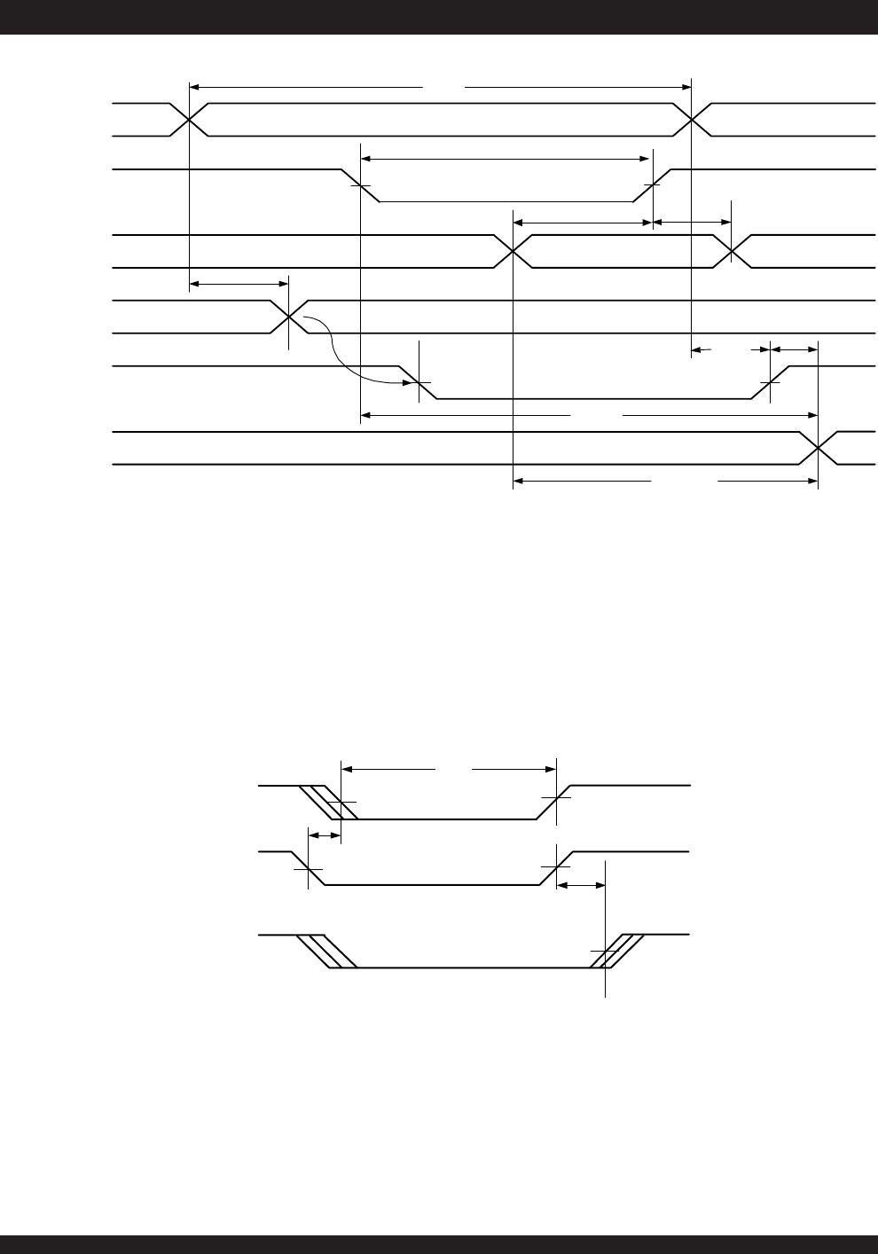
1. Port-to-port delay through RAM cells from writing port to reading port, refer to "Timing Waveform of Write with Port-to-Port Read and BUSY (M/S = V
IH)".
2. To ensure that the earlier of the two ports wins.
3. t
BDD is a calculated parameter and is the greater of the Max. spec, tWDD – tWP (actual), or tDDD – tDW (actual).
4. To ensure that the write cycle is inhibited on port "B" during contention on port "A".
5. To ensure that a write cycle is completed on port "B" after contention on port "A".
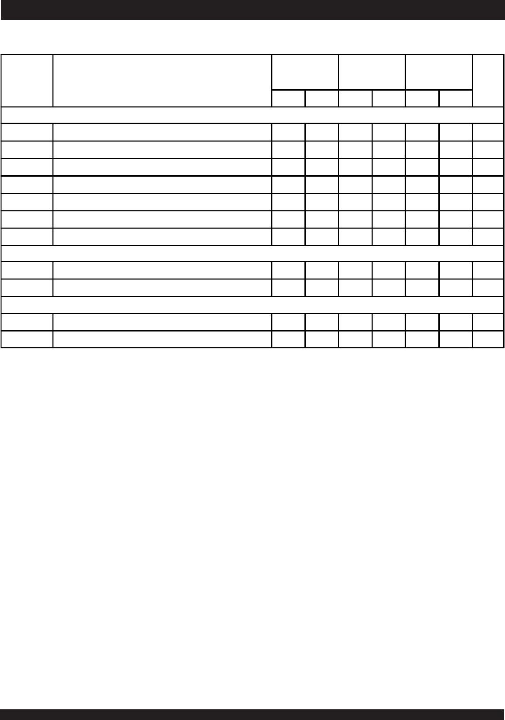
AC Electrical Characteristics Over the
Operating Temperature and Supply Voltage Range
Symbol Parameter
70V631S10
Com'l Only
70V631S12
Com'l
& Ind
70V631S15
Com'l
Unit
Min. Max. Min. Max. Min. Max.
BUSY TIMING (M/S=V
IH
)
t
BAA
BUSY Access Time from Address Match
____
10
____
12
____
15 ns
t
BDA
BUSY Disable Time from Address Not Matched
____
10
____
12
____
15 ns
t
BAC
BUSY Access Time from Chip Enable Low
____
10
____
12
____
15 ns
t
BDC
BUSY Disable Time from Chip Enable High
____
10
____
12
____
15 ns
t
APS
Arbitration Priority Set-up Time
(2 )
5
____
5
____
5
____
ns
t
BDD
BUSY Disable to Valid Data
(3)
____
10
____
12
____
15 ns
t
WH
Write Hold After BUSY
(5)
8
____
10
____
12
____
ns
BUSY TIMING (M/S=V
IL
)
t
WB
BUSY Input to Write
(4 )
0
____
0
____
0
____
ns
t
WH
Write Hold After BUSY
(5)
8
____
10
____
12
____
ns
PORT-TO-PORT DELAY TIMING
t
WDD
Write Pulse to Data Delay
(1 )
____
22
____
25
____
30 ns
t
DDD
Write Data Valid to Read Data Delay
(1 )
____
20
____
22
____
25 ns
5622 tbl 14