N74F280BD,602

Philips Semiconductors Product specification
74F280B9-bit odd/even parity generator/checker
1996 Mar 12
4
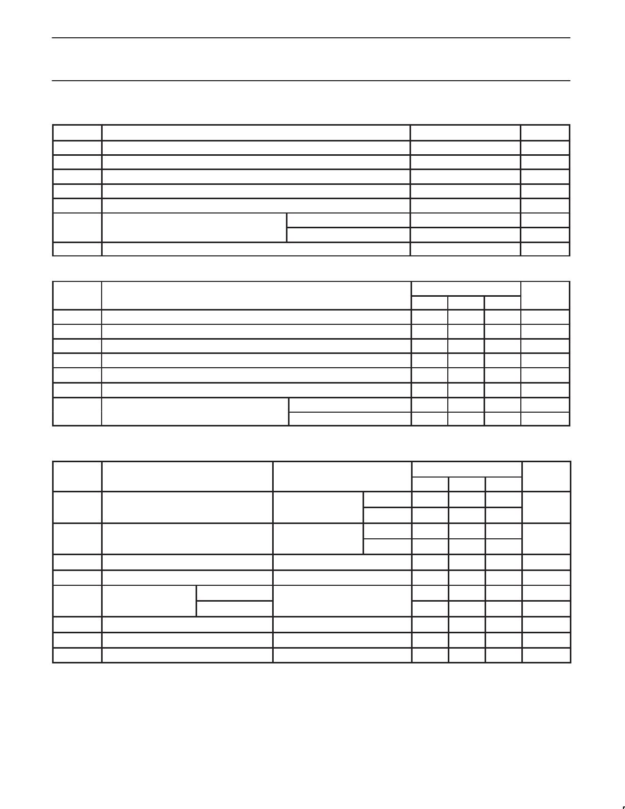
ABSOLUTE MAXIMUM RATINGS
SYMBOL PARAMETER RATING UNIT
V
CC
Supply voltage –0.5 to +7.0 V
V
IN
Input voltage –0.5 to +7.0 V
I
IN
Input current –30 to +5 mA
V
OUT
Voltage applied to output in High output state –0.5 to V
CC
V
I
OUT
Current applied to output in Low output state 40 mA
T
O
p
erating free air tem
p
erature range
Commercial range 0 to +70 °C
T
amb
Operating
free
-
air
temperat
u
re
range
Industrial range –40 to +85 °C
T
stg
Storage temperature –65 to +150 °C
RECOMMENDED OPERATING CONDITIONS
SYMBOL
PARAMETER
LIMITS
UNIT
SYMBOL
PARAMETER
Min Nom Max
UNIT
V
CC
Supply voltage 4.5 5.0 5.5 V
V
IH
High-level input voltage 2.0 V
V
IL
Low-level input voltage 0.8 V
I
IK
Input clamp current –18 mA
I
OH
High-level output current –1
mA
I
OL
Low-level output current 20 mA
T
O
p
erating free air tem
p
erature range
Commercial range 0 70 °C
T
amb
Operating
free
-
air
temperat
u
re
range
Industrial range –40 85 °C
DC ELECTRICAL CHARACTERISTICS
(Over recommended operating free-air temperature range unless otherwise noted.)
SYMBOL
PARAMETER
TEST CONDITIONS
1
LIMITS
UNIT
SYMBOL
PARAMETER
TEST
CONDITIONS
1
MIN TYP
2
MAX
UNIT
V
O
High level out
p
ut voltage
V
CC
= MIN, V
IL
= MAX ±10%V
CC
2.5
V
V
OH
High
-
le
v
el
o
u
tp
u
t
v
oltage
V
IH
= MIN, I
OH
= MAX ±5%V
CC
2.7 3.4
V
V
O
Low level out
p
ut voltage
V
CC
= MIN, V
IL
= MAX ±10%V
CC
0.35 0.50
V
V
OL
Lo
w-
le
v
el
o
u
tp
u
t
v
oltage
V
IH
= MIN, I
OL
= MAX ±5%V
CC
0.35 0.50
V
V
IK
Input clamp voltage V
CC
= MIN, I
I
= I
IK
–0.73 –1.2 V
I
I
Input current at maximum input voltage V
CC
= 0.0V, V
I
= 7.0V 100 µA
I
High level in
p
ut current
Commercial range
V
CC
= MAX V =27V
20 µA
I
IH
High
-
le
v
el
inp
u
t
c
u
rrent
Industrial range
V
CC
=
MAX
,
V
I
=
2
.
7V
40 µA
I
IL
Low-level input current V
CC
= MAX, V
I
= 0.5V –20 µA
I
OS
Short-circuit output current
3
V
CC
= MAX –60 –150 mA
I
CC
Supply current (total) V
CC
= MAX 26 35 mA
NOTES:
1. For conditions shown as MIN or MAX, use the appropriate value specified under recommended operating conditions for the applicable type.
2. All typical values are at V
CC
= 5V, T
amb
= 25°C.
3. Not more than one output should be shorted at a time. For testing I
OS
, the use of high-speed test apparatus and/or sample-and-hold
techniques are preferable in order to minimize internal heating and more accurately reflect operational values. Otherwise, prolonged shorting
of a High output may raise the chip temperature well above normal and thereby cause invalid readings in other parameter tests. In any
sequence of parameter tests, I
OS
tests should be performed last.
Philips Semiconductors Product specification
74F280B9-bit odd/even parity generator/checker
1996 Mar 12
5
AC ELECTRICAL CHARACTERISTICS
LIMITS
T
amb
= +25°C
V =+5V
T
amb
= 0°C to +70°C
V =+5V± 10%
T
amb
= -40°C to +85°C
V =+5V± 10%
SYMBOL PARAMETER
V
CC
= +
5
.
V
C
L
= 50
p
F
,
V
CC
= +
5
.
V
±
10%
C
L
= 50
p
F
,
V
CC
= +
5
.
V
±
10%
C
L
= 50
p
F
,
UNIT
C
L
=
50pF,
R
L
= 500
C
L
=
50pF,
R
L
= 500
C
L
=
50pF,
R
L
= 500
Min Typ Max Min Max Min Max
t
PLH
t
PHL
Propagation delay
I
0
- I
8
to Σ
E
74F280B
Waveform 1, 2
4.0
4.0
6.5
7.0
9.0
10.0
3.5
3.5
10.0
11.1
3.0
3.5
11.0
12.0
ns
ns
t
PLH
t
PHL
Propagation delay
I
0
- I
8
to Σ
O
74F280B
Waveform 1, 2
4.0
4.0
6.5
7.0
9.0
10.0
3.5
3.5
10.0
11.0
3.0
3.5
11.0
12.0
ns
ns
AC WAVEFORMS
For all waveforms, V
M
=1.5V.
V
M
V
M
V
M
V
M
I
0
- I
8
Σ
E,
Σ
O
t
PHL
t
PLH
SF00848
Waveform 1. Propagation Delay for Inverting Outputs
V
M
V
M
V
M
V
M
I
0
- I
8
Σ
E,
Σ
O
t
PLH
t
PHL
SF00850
Waveform 2. Propagation Delay for Non-Inverting Outputs
TEST CIRCUIT AND WAVEFORM
t
w
90%
V
M
10%
90%
V
M
10%
90%
V
M
10%
90%
V
M
10%
NEGATIVE
PULSE
POSITIVE
PULSE
t
w
AMP (V)
0V
0V
t
THL
(
t
f
)
INPUT PULSE REQUIREMENTS
rep. rate
t
w
t
TLH
t
THL
1MHz 500ns
2.5ns 2.5ns
Input Pulse Definition
V
CC
family
74F
D.U.T.
PULSE
GENERATOR
R
L
C
L
R
T
V
IN
V
OUT
Test Circuit for Totem-Pole Outputs
DEFINITIONS:
R
L
= Load resistor;
see AC ELECTRICAL CHARACTERISTICS for value.
C
L
= Load capacitance includes jig and probe capacitance;
see AC ELECTRICAL CHARACTERISTICS for value.
R
T
= Termination resistance should be equal to Z
OUT
of
pulse generators.
t
THL
(
t
f
)
t
TLH
(
t
r
)
t
TLH
(
t
r
)
AMP (V)
amplitude
3.0V 1.5V
V
M
SF00006
Philips Semiconductors Product specification
74F280B
9-bit parity odd/even parity generator/checker
1996 Mar 12
6
DIP14: plastic dual in-line package; 14 leads (300 mil) SOT27-1

N74F280BD,602

Mfr. #:
Manufacturer:
NXP Semiconductors
Description:
Parity Functions 9-BIT ODD/EVEN PAR
Lifecycle:
New from this manufacturer.
Delivery:
DHL FedEx Ups TNT EMS
Payment:
T/T Paypal Visa MoneyGram Western Union

Products related to this Datasheet