AC Timing Adjustments
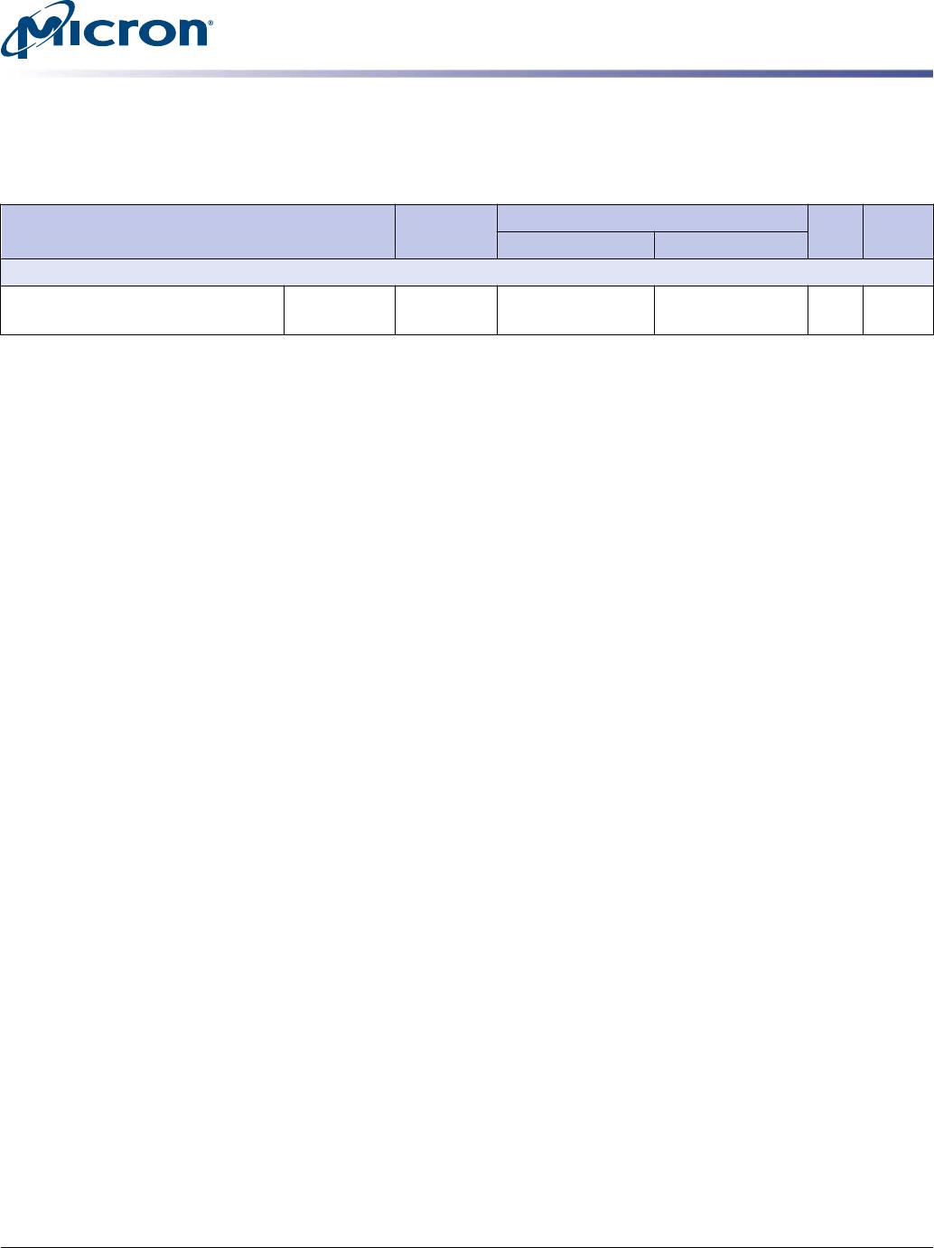
Table 3: Electrical Characteristics and AC Operating Conditions for Speed Extensions
Notes 1–8 apply to the entire table
Parameter Symbol
DDR3-2133
Unit NotesMin Max
Command and Address Timing
Four ACTIVATE windows 2KB page
size
t
FAW 30 – ns 9
Notes:
1. AC timing parameters are valid from specified T
C
MIN to T
C
MAX values.
2. All voltages are referenced to V
SS
.
3. Output timings are only valid for R
ON34
output buffer selection.
4. The unit
t
CK (AVG) represents the actual
t
CK (AVG) of the input clock. The unit CK repre-
sents one clock cycle of the input clock, counting the actual clock edges.
5. AC timing and I
DD
tests may use a V
IL
-to-V
IH
swing of up to 900mV in the test environ-
ment, but input timing is still referenced to V
REF
(except
t
IS,
t
IH,
t
DS, and
t
DH use the
AC/DC trip points and CK, CK# and DQS, DQS# use their crossing points). The minimum
slew rate for the input signals used to test the device is 1 V/ns for single-ended inputs
(DQs are at 2V/ns for DDR3-1866 and DDR3-2133) and 2 V/ns for differential inputs in
the range between V
IL(AC)
and V
IH(AC)
.
6. All timings that use time-based values (ns, µs, ms) should use
t
CK (AVG) to determine the
correct number of clocks (Table 3 (page 3) uses CK or
t
CK [AVG] interchangeably). In the
case of noninteger results, all minimum limits are to be rounded up to the nearest
whole integer, and all maximum limits are to be rounded down to the nearest whole
integer.
7. Strobe or DQSdiff refers to the DQS and DQS# differential crossing point when DQS is
the rising edge. Clock or CK refers to the CK and CK# differential crossing point when
CK is the rising edge.
8. This output load is used for all AC timing (except ODT reference timing) and slew rates.
The actual test load may be different. The output signal voltage reference point is
V
DDQ
/2 for single-ended signals and the crossing point for differential signals.
9. For these parameters, the DDR3 SDRAM device supports
t
nPARAM (nCK) = RU(
t
PARAM
[ns]/
t
CK[AVG] [ns]), assuming all input clock jitter specifications are satisfied. For exam-
ple, the device will support
t
nRP (nCK) = RU(
t
RP/
t
CK[AVG]) if all input clock jitter specifi-
cations are met. This means that for DDR3-800 6-6-6, of which
t
RP = 5ns, the device will
support
t
nRP = RU(
t
RP/
t
CK[AVG]) = 6 as long as the input clock jitter specifications are
met. That is, the PRECHARGE command at T0 and the ACTIVATE command at T0 + 6 are
valid even if six clocks are less than 15ns due to input clock jitter.
8000 S. Federal Way, P.O. Box 6, Boise, ID 83707-0006, Tel: 208-368-3900
www.micron.com/productsupport Customer Comment Line: 800-932-4992
Micron and the Micron logo are trademarks of Micron Technology, Inc.
All other trademarks are the property of their respective owners.
This data sheet contains minimum and maximum limits specified over the power supply and temperature range set forth herein.
Although considered final, these specifications are subject to change, as further product development and data characterization some-
times occur.
4Gb: x16 DDR3 SDRAM Reduced tFAW Addendum
AC Timing Adjustments
PDF: 09005aef857c6ed1
4Gb_DDR3_SDRAM_tFAW.pdf - Rev. B 3/14 EN
3
Micron Technology, Inc. reserves the right to change products or specifications without notice.
© 2013 Micron Technology, Inc. All rights reserved.

