PCA9538 All information provided in this document is subject to legal disclaimers. © NXP Semiconductors N.V. 2017. All rights reserved.
Product data sheet Rev. 8 — 8 November 2017 7 of 34
NXP Semiconductors
PCA9538
8-bit I
2
C-bus and SMBus low power I/O port with interrupt and reset
6.2.3 Register 1 - Output Port register
This register reflects the outgoing logic levels of the pins defined as outputs by Register 3.
Bit values in this register have no effect on pins defined as inputs. Reads from this register
return the value that is in the flip-flop controlling the output selection, not the actual pin
value.
6.2.4 Register 2 - Polarity Inversion register
This register allows the user to invert the polarity of the Input Port register data. If a bit in
this register is set (written with 1), the corresponding Input Port data is inverted. If a bit in
this register is cleared (written with a 0), the Input Port data polarity is retained.
Table 6. Register 1 - Output Port register bit description
Legend: * default value.
Bit Symbol Access Value Description
7 O7 R 1* reflects outgoing logic levels of pins defined as outputs
by Register 3
6O6 R 1*
5O5 R 1*
4O4 R 1*
3O3 R 1*
2O2 R 1*
1O1 R 1*
0O0 R 1*
Table 7. Register 2 - Polarity Inversion register bit description
Legend: * default value.
Bit Symbol Access Value Description
7 N7 R/W 0* inverts polarity of Input Port register data
0 = Input Port register data retained (default value)
1 = Input Port register data inverted
6N6 R/W0*
5N5 R/W0*
4N4 R/W0*
3N3 R/W0*
2N2 R/W0*
1N1 R/W0*
0N0 R/W0*
PCA9538 All information provided in this document is subject to legal disclaimers. © NXP Semiconductors N.V. 2017. All rights reserved.
Product data sheet Rev. 8 — 8 November 2017 8 of 34
NXP Semiconductors
PCA9538
8-bit I
2
C-bus and SMBus low power I/O port with interrupt and reset
6.2.5 Register 3 - Configuration register
This register configures the directions of the I/O pins. If a bit in this register is set, the
corresponding port pin is enabled as an input with high-impedance output driver. If a bit in
this register is cleared, the corresponding port pin is enabled as an output. At reset, the
I/Os are configured as inputs.
6.3 Power-on reset
When power is applied to V
DD
, an internal Power-On Reset (POR) holds the PCA9538 in
a reset condition until V
DD
has reached V
POR
. At that point, the reset condition is released
and the PCA9538 registers and state machine will initialize to their default states.
Thereafter, V
DD
must be lowered below 0.2 V to reset the device.
For a power reset cycle, V
DD
must be lowered below 0.2 V and then restored to the
operating voltage.
6.4 RESET input
A reset can be accomplished by holding the RESET pin LOW for a minimum of t
w(rst)
.
The PCA9538 registers and SMBus/I
2
C-bus state machine will be held in their default
state until the RESET
input is once again HIGH. This input requires a pull-up resistor to
V
DD
if no active connection is used.
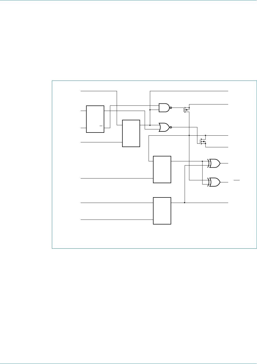
6.5 Interrupt output
The open-drain interrupt output (INT) is activated when one of the port pins changes state
and the pin is configured as an input. The interrupt is de-activated when the input returns
to its previous state or the Input Port register is read.
Note that changing an I/O from an output to an input may cause a false interrupt to occur
if the state of the pin does not match the contents of the Input Port register.
Table 8. Register 3 - Configuration register bit description
Legend: * default value.
Bit Symbol Access Value Description
7 C7 R/W 1* configures the directions of the I/O pins
0 = corresponding port pin enabled as an output
1 = corresponding port pin configured as an input
(default value)
6C6 R/W 1*
5C5 R/W 1*
4C4 R/W 1*
3C3 R/W 1*
2C2 R/W 1*
1C1 R/W 1*
0C0 R/W 1*
PCA9538 All information provided in this document is subject to legal disclaimers. © NXP Semiconductors N.V. 2017. All rights reserved.
Product data sheet Rev. 8 — 8 November 2017 9 of 34
NXP Semiconductors
PCA9538
8-bit I
2
C-bus and SMBus low power I/O port with interrupt and reset
6.6 I/O port
When an I/O is configured as an input, FETs Q1 and Q2 are off, creating a
high-impedance input. The input voltage may be raised above V
DD
to a maximum of 5.5 V.
If the I/O is configured as an output, then either Q1 or Q2 is enabled, depending on the
state of the Output Port register. Care should be exercised if an external voltage is applied
to an I/O configured as an output because of the low-impedance paths that exist between
the pin and either V
DD
or V
SS
.
Remark: At power-on reset, all registers return to default values.
Fig 6. Simplified schematic of IO0 to IO7
V
DD
I/O pin
output port
register data
configuration
register
DQ
CK Q
data from
shift register
write
configuration
pulse
output port
register
DQ
CK
write pulse
polarity inversion
register
DQ
CK
data from
shift register
write polarity
pulse
input port
register
DQ
CK
read pulse
input port
register data
polarity
inversion
register data
002aad723
FF
data from
shift register
FF
FF
FF
Q1
Q2
V
SS
to INT

PCA9538PW/Q900,118

Mfr. #:
Manufacturer:
NXP Semiconductors
Description:
Interface - I/O Expanders 8b I2C BUS INTERUPT
Lifecycle:
New from this manufacturer.
Delivery:
DHL FedEx Ups TNT EMS
Payment:
T/T Paypal Visa MoneyGram Western Union