Micropower
Quad-Channel Digital Isolators
Data Sheet
ADuM1440/ADuM1441/ADuM1442/ADuM1445/ADuM1446/ADuM1447
Rev. E Document Feedback
Information furnished by Analog Devices is believed to be accurate and reliable. However, no
responsibility is assumed by Analog Devices for its use, nor for any infringements of patents or other
rights of third parties that may result from its use. Specifications subject to change without notice. No
license is granted by implication or otherwise under any patent or patent rights of Analog Devices.
Trademarks and registered trademarks are the property of their respective owners.
One Technology Way, P.O. Box 9106, Norwood, MA 02062-9106, U.S.A.
Tel: 781.329.4700 ©2013–2017 Analog Devices, Inc. All rights reserved.
Technical Support www.analog.com
FEATURES
Ultralow power operation
3.3 V operation (typical)
5.6 μA per channel quiescent current, refresh enabled
0.3 μA per channel quiescent current, refresh disabled
148 μA/Mbps per channel typical dynamic current
2.5 V operation (typical)
3.1 μA per channel quiescent current, refresh enabled
0.1 μA per channel quiescent current, refresh disabled
117 μA/Mbps per channel typical dynamic current
Small, 16-lead QSOP and 20-Lead SSOP
Bidirectional communication
Up to 2 Mbps data rate (NRZ)
High temperature operation: 125°C
High common-mode transient immunity: >25 kV/μs
Safety and regulatory approvals
UL 1577 component recognition program
2500 V rms for 1 minute per UL 1577 QSOP package
3750V rms for 1 minute per UL 1577 SSOP package
CSA Component Acceptance Notice 5A
VDE certificate of conformity
DIN V VDE V 0884-10 (VDE V 0884-10):2006-12
V
IORM
= 565 V
PEAK
QSOP package
V
IORM
= 849 V
PEAK
SSOP package
IECEx and ATEX intrinsic safety
Sira 0518 II 1G Ex ia IIC Ga
APPLICATIONS
General-purpose, low power multichannel isolation
1 MHz, low power peripheral interface (SPI)
4 mA to 20 mA loop process controls
GENERAL DESCRIPTION
The ADuM1440/ADuM1441/ADuM1442/ADuM1445/
ADuM1446/ADuM1447
1
are micropower, 4-channel digital
isolators based on the Analog Devices, Inc., iCoupler® technology.
Combining high speed, complementary metal oxide semiconductor
(CMOS) and monolithic air core transformer technologies,
these isolation components provide outstanding performance
characteristics superior to the alternatives, such as optocoupler
devices. As shown in Figure 3, in standard operating mode,
when EN
x
= 0 (internal refresh enabled), the current per channel is
less than 10 μA. When EN
x
= 1 (internal refresh disabled), the
current per channel drops to less than 1 μA.
The ADuM1440/ADuM1441/ADuM1442/ADuM1445/
ADuM1446/ADuM1447 family of quad 2.5 kV digital isolation
devices are packaged in a small 16-lead QSOP and 20-lead SSOP,
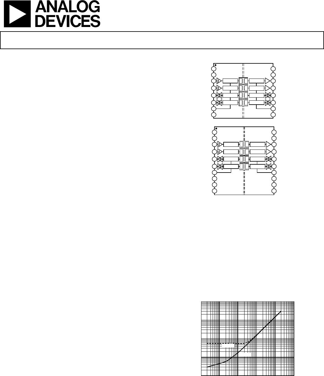
FUNCTIONAL BLOCK DIAGRAMS
ENCODE DECODE
ENCODE DECODE
ENCODE DECODE
ENCODE DECODE
V
DD1
GND
1
V
IA
V
IB
V
IC
/V
OC
V
ID
/V
OD
EN
1
GND
1
V
DD2
GND
2
V
OA
V
OB
V
OC
/V
IC
V
OD
/V
ID
EN
2
GND
2
1
2
3
4
5
6
7
8
16
15
14
13
12
11
10
9
ADuM144x QSOP
11845-002
Figure 1.
ENCODE DECODE
ENCODE DECODE
ENCODE DECODE
V
DD1
GND
1
V
IA
V
IB
V
IC
/V
OC
V
ID
/V
OD
EN
1
NIC
V
DD2
GND
2
V
OA
V
OB
V
OC
/V
IC
V
OD
/V
ID
EN
2
NIC
1
2
3
4
5
7
8
20
19
18
17
16
14
13
NIC
GND
1
NIC
GND
2
9
10
12
11
ADuM144x
ENCODE DECODE
6 15
11845-102
Figure 2.
freeing almost 70% of board space compared to isolators packages
in wide body SOIC packages.
The devices withstand high isolation voltages and meet regulatory
requirements, such as UL and CSA standards. In addition to the
space savings, the ADuM1440/ADuM1441/ADuM1442/
ADuM1445/ADuM1446/ADuM1447 operate with supplies as
low as 2.25 V.
Despite the low power consumption, all models of the ADuM1440/
ADuM1441/ADuM1442/ADuM1445/ADuM1446/ADuM1447
provide low, pulse width distortion at <8 ns. In addition, every
model has an input glitch filter to protect against extraneous
noise disturbances.
0.1
1
10
100
1000
0.1 1 10 100 1000 10000
CURRENT PER CHANNEL
(
µA)
DATA RATE (kbps)
EN
x
= 1
EN
x
= 0
11845-001
Figure 3. Typical Total Supply Current per Channel (V
DDx
= 3.3 V)
1
Protected by U.S. Patents 5,952,849, 6,873,065, 7,075,329, 6,262,600. Other patents pending.
ADuM1440/ADuM1441/ADuM1442/ADuM1445/ADuM1446/ADuM1447 Data Sheet
Rev. E | Page 2 of 25
TABLE OF CONTENTS
Features .............................................................................................. 1
Applications ....................................................................................... 1
General Description ......................................................................... 1
Functional Block Diagrams ............................................................. 1
Revision History ............................................................................... 2
Specifications ..................................................................................... 3
Electrical Characteristics—3.3 V Operation ............................ 3
Electrical Characteristics—2.5 V Operation ............................ 5
Electrical Characteristics—V
DD1
= 3.3 V, V
DD2
= 2.5 V
Operation ....................................................................................... 7
Electrical Characteristics—V
DD1
= 2.5 V, V
DD2
= 3.3 V
Operation ....................................................................................... 8
Package Characteristics ............................................................... 9
Regulatory Information ............................................................... 9
Insulation and Safety Related Specifications .......................... 10
DIN V VDE V 0884-10 (VDE V 0884-10):2006-12 Insulation
Characteristics ............................................................................ 10
Intrinsic Safety ............................................................................ 11
Absolute Maximum Ratings ......................................................... 13
ESD Caution................................................................................ 13
Pin Configurations and Function Descriptions ......................... 14
Typical Performance Characteristics ........................................... 17
Applications Information .............................................................. 20
PCB Layout ................................................................................. 20
Propagation Delay-Related Parameters ................................... 20
DC Correctness ............................................................................ 20
Magnetic Field Immunity ............................................................. 21
Power Consumption .................................................................. 22
Insulation Lifetime ..................................................................... 22
Outline Dimensions ....................................................................... 24
Ordering Guide .......................................................................... 25
REVISION HISTORY
1/2017—Rev. D to Rev. E
Changes to Features Section............................................................ 1
Changes to Table 12 .......................................................................... 9
Added Intrinsic Safety Section, Table 16; Renumbered Sequentially,
and Table 17 ..................................................................................... 11
4/2015—Rev. C to Rev. D
Change to General Description Section ........................................ 1
4/2015—Rev. B to Rev. C
Changes to Regulatory Information Section ................................ 9
3/2015—Rev. A to Rev. B
Changes to Features Section and Figure 3 ..................................... 1
Changes to Table 12 .......................................................................... 9
Changes to Table 13 and Table 14 ................................................ 10
Updated Outline Dimensions ....................................................... 23
Changes to Ordering Guide .......................................................... 24
3/2014—Rev. 0 to Rev. A
Added SSOP Package ......................................................... Universal
Changes to Features Section, Added Figure 2,
Renumbered Sequentially ................................................................ 1
Changes to Output Voltage Logic High Parameter, Table 3 ........ 4
Added Table 15, Renumbered Sequentially; Changes to
Figure 4 ............................................................................................ 11
Change to Supply Voltages (V
DD1
, V
DD2
) Parameter, Table 17 ........ 12
Added Figure 6; Changes to Table 20 .......................................... 13
Added Figure 8; Changes to Table 21 .......................................... 14
Added Figure 10, Changes to Table 22 ........................................ 15
Added Figure 30 ............................................................................. 19
Changes to Power Consumption Section; Added Table 23 ...... 21
Added Figure 27 ............................................................................. 23
Changes to Ordering Guide .......................................................... 24
10/2013—Revision 0: Initial Version
Data Sheet ADuM1440/ADuM1441/ADuM1442/ADuM1445/ADuM1446/ADuM1447
Rev. E | Page 3 of 25
SPECIFICATIONS
ELECTRICAL CHARACTERISTICS3.3 V OPERATION
All typical specifications are at T
A
= 25°C, V
DD1
= V
DD2
= 3.3 V. Minimum/maximum specifications apply over the entire recommended
operating range of 3.0 V ≤ V
DD1
≤ 3.6 V, 3.0 V ≤ V
DD2
3.6 V, and 40°C T
A
≤ +125°C, unless otherwise noted. Switching specifications
are tested with C
L
= 15 pF, and CMOS signal levels, unless otherwise noted.
Table 1.
Parameter
Symbol
Min
Typ
Max
Unit
SWITCHING SPECIFICATIONS
Data Rate
2
Mbps
Propagation Delay t
PHL
, t
PLH
80 180 ns 50% input to 50% output
Change vs. Temperature 200 ps/°C
Minimum Pulse Width PW 500 ns Within PWD limit
Pulse-Width Distortion PWD 8 ns |t
PLH
− t
PHL
|
Propagation Delay Skew
1
t
PSK
10 ns
Channel Matching
Codirectional t
PSKCD
10 ns
Opposing Direction t
PSKOD
15 ns
1
t
PSK
is the magnitude of the worst-case difference in t
PHL
and t
PLH
that is measured between units at the same operating temperature, supply voltages, and output load within the
recommended operating conditions.
Table 2.
Parameter Symbol Min Typ Max Unit Test Conditions/Comments
SUPPLY CURRENT 2 Mbps, no load
ADuM1440/ADuM1445 I
DD1
732 1000 µA EN
X
= 0 V, V
IH
= V
DD
, V
IL
= 0 V
I
DD2
492 750 µA EN
X
= 0 V, V
IH
= V
DD
, V
IL
= 0 V
ADuM1441/ADuM1446 I
DD1
672 900 µA EN
X
= 0 V, V
IH
= V
DD
, V
IL
= 0 V
I
DD2
552 900 µA EN
X
= 0 V, V
IH
= V
DD
, V
IL
= 0 V
ADuM1442/ADuM1447 I
DD1
612 900 µA EN
X
= 0 V, V
IH
= V
DD
, V
IL
= 0 V
I
DD2
612 900 µA EN
X
= 0 V, V
IH
= V
DD
, V
IL
= 0 V

ADUM1446ARSZ-RL7

Mfr. #:
Manufacturer:
Analog Devices Inc.
Description:
Digital Isolators Micro-power Quad-CH Digital Isolator
Lifecycle:
New from this manufacturer.
Delivery:
DHL FedEx Ups TNT EMS
Payment:
T/T Paypal Visa MoneyGram Western Union