ADuM1440/ADuM1441/ADuM1442/ADuM1445/ADuM1446/ADuM1447 Data Sheet
Rev. E | Page 16 of 25
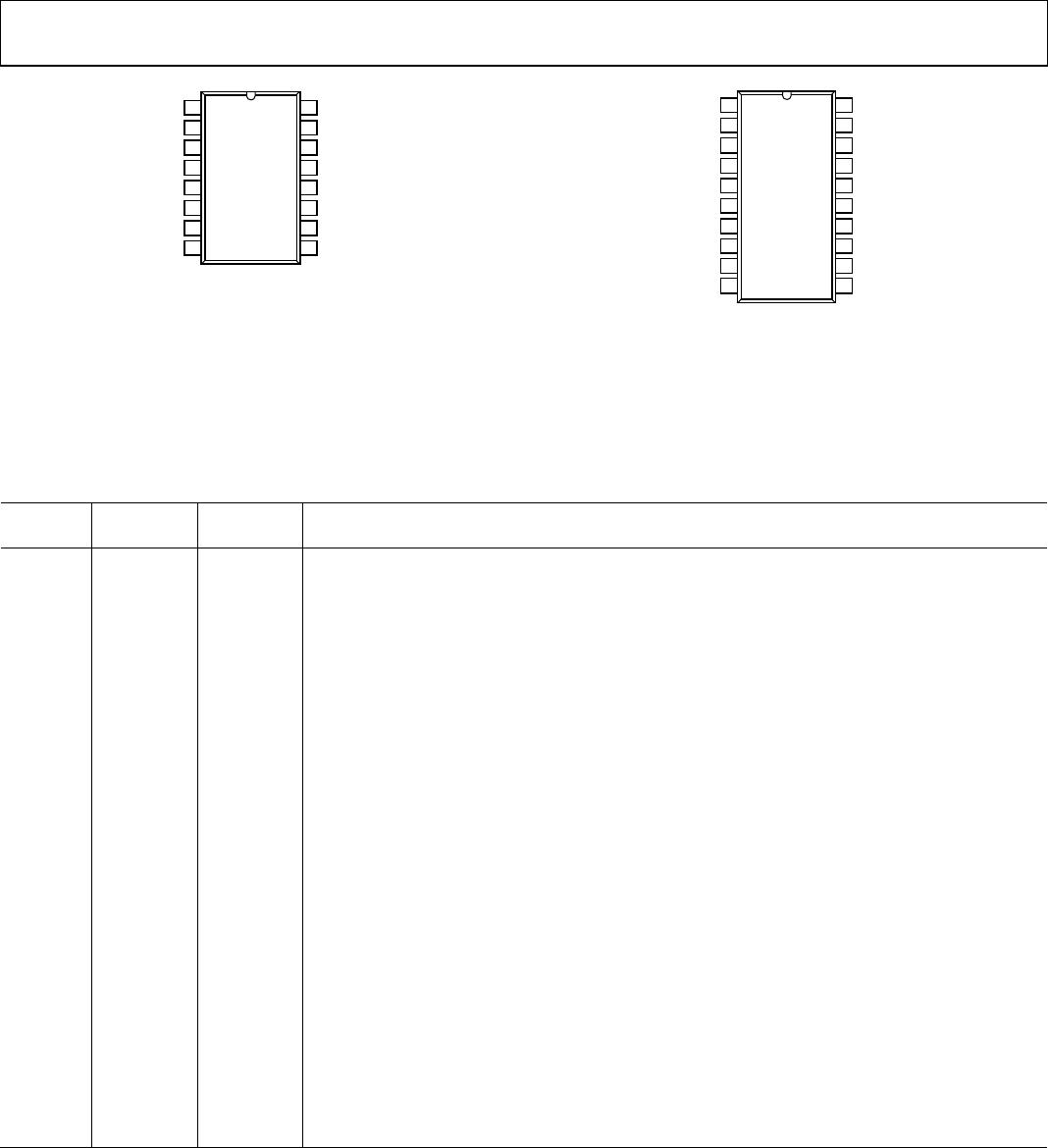
V
DD1
1
GND
1
1
2
V
IA
3
V
IB
4
V
DD2
16
GND
2
2
15
V
OA
14
V
OB
13
V
OC
5
V
IC
12
V
OD
6
V
ID
11
EN
1
7
EN
2
10
GND
1
1
8
GND
2
2
9
ADuM1442/
ADuM1447
TOP VIEW
(Not to Scale)
1
PIN 2 AND PIN 8 ARE INTERNALLY CONNECTED. CONNECTING BOTH
TO GND
1
IS RECOMMENDED.
2
PIN 9 AND PIN 15 ARE INTERNALLY CONNECTED. CONNECTING
BOTH TO GND
2
IS RECOMMENDED.
11845-006
Figure 9. ADuM1442/ADuM1447 QSOP Pin Configuration
V
DD1
1
GND
1
1
2
V
IA
3
V
IB
4
V
DD2
NIC = NOT INTERNALLY CONNECTED.
20
GND
2
2
19
V
OA
18
V
OB
17
V
OC
5
V
IC
16
V
OD
6
V
ID
15
EN
1
7
EN
2
14
NIC
8
NIC
13
NIC
9
NIC
12
GND
1
1
10
GND
2
2
11
ADuM1442/
ADuM1447
TOP VIEW
(Not to Scale)
11845-110
1
PIN 2 AND PIN 10 ARE INTERNALLY CONNECTED.
CONNECTING BOTH TO GND
1
IS RECOMMENDED.
2
PIN 11 AND PIN 19 ARE INTERNALLY CONNECTED.
CONNECTING BOTH TO GND
2
IS RECOMMENDED.
Figure 10. ADuM1442/ADuM1447 SSOP Pin Configuration
Table 24. ADuM1442/ADuM1447 Pin Function Descriptions
1
QSOP
Pin No.
2
SSOP
Pin No. Mnemonic Description
1 1 V
DD1
Supply Voltage for Isolator Side 1 (2.25 V to 3.6 V). Connect a ceramic bypass capacitor in the 0.01
µF to 0.1 µF range between V
DD1
(Pin 1) and GND
1
(Pin 2).
2, 8 2, 10 GND
1
Ground 1. Ground reference for Isolator Side 1. Pin 2 and Pin 8 are internally connected, and connecting
both to GND
1
is recommended.
3 3 V
IA
Logic Input A.
4 4 V
IB
Logic Input B.
5 5 V
OC
Logic Output C.
6 3 V
OD
Logic Output D.
7 7 EN
1
Refresh/Watchdog Enable 1. Connecting Pin 7 to GND
1
enables input/output refresh and
watchdog functionality for Side 1, supporting standard iCoupler operation. Tying Pin 7 to V
DD1
disables refresh and watchdog functionality for lowest power operation, see the Applications
Information section for detailed description of this mode. EN
1
and EN
2
must be set to the same
logic state.
9, 15 11, 19 GND
2
Ground 2. Ground reference for Isolator Side 2. Pin 9 and Pin 15 are internally connected, and
connecting both to GND
2
is recommended.
10 14 EN
2
Refresh/Watchdog Enable 2. Connecting Pin 10 to GND
2
enables input/output refresh and
watchdog functionality for Side 2, supporting standard iCoupler operation. Tying Pin 10 to V
DD2
disables refresh and watchdog functionality for lowest power operation, see the Applications
Information section for a detailed description of this mode. EN
1
and EN
2
must be set to the same
logic state.
11
15
V
ID
Logic Input D.
12 16 V
IC
Logic Input C.
13 17 V
OB
Logic Output B.
14 18 V
OA
Logic Output A.
16 20 V
DD2
Supply Voltage for Isolator Side 2 (2.25 V to 3.6 V). Connect a ceramic bypass capacitor in the 0.01
µF to 0.1 µF range between V
DD2
(Pin 16) and GND
2
(Pin 15).
N/A
8, 9, 12, 13
NC
No Connect. Do not connect to this pin.
1
Reference the AN-1109 Application Note for specific layout guidelines.
2
N/A = not applicable.
Data Sheet ADuM1440/ADuM1441/ADuM1442/ADuM1445/ADuM1446/ADuM1447
Rev. E | Page 17 of 25
TYPICAL PERFORMANCE CHARACTERISTICS
0
50
100
150
200
250
300
350
0 500 1000 1500 2000
CURRENT CONSUMPTION PER INPUT (µA)
DATA RATE (kbps)
V
DDx
INPUT CURRENT
11845-007
0
5
10
15
0 20 40
Figure 11. Current Consumption per Input vs. Data Rate for 2.5 V,
EN
x
= Low Operation
0
10
20
30
40
50
60
70
80
90
0 500 1000 1500 2000
CURRENT CONSUMPTION PER OUTPUT (µA)
DATA RATE (kbps)
V
DDx
OUTPUT CURRENT
11845-008
0
2
4
0 20 40
Figure 12. Current Consumption per Output vs. Data Rate for 2.5 V,
EN
x
= Low Operation
0
50
100
150
200
250
300
350
400
0 500 1000 1500 2000
CURRENT CONSUMPTION PER INPUT (µA)
DATA RATE (kbps)
V
DDx
INPUT CURRENT
11845-009
0
5
10
15
0 20 40
Figure 13. Current Consumption per Input vs. Data Rate for 3.3 V,
EN
x
= Low Operation
0
20
40
60
80
100
120
140
0 500 1000 1500
2000
CURRENT CONSUMPTION PER OUTPUT (µA)
DATA RATE (kbps)
V
DDx
OUTPUT CURRENT
11845-010
0
2
4
0 20 40
Figure 14. Current Consumption per Output vs. Data Rate for 3.3 V,
EN
x
= Low Operation
0
20
40
60
80
100
120
140
160
0 500 1000 1500 2000
CURRENT CONSUMPTION PER INPUT (µA)
DATA RATE (kbps)
V
DDx
INPUT CURRENT
11845-01
1
0
0.5
1.0
0
5 10
Figure 15. Current Consumption per Input vs. Data Rate for 2.5 V,
EN
x
= High Operation
0
10
20
30
40
50
60
70
80
90
0 500 1000 1500 2000
CURRENT CONSUMPTION PER OUTPUT (µA)
DATA RATE (kbps)
V
DDx
OUTPUT CURRENT
11845-012
0
0.5
1.0
0 5 10
Figure 16. Current Consumption per Output vs. Data Rate for 2.5 V,
EN
x
= High Operation
ADuM1440/ADuM1441/ADuM1442/ADuM1445/ADuM1446/ADuM1447 Data Sheet
Rev. E | Page 18 of 25
0
20
60
40
100
80
120
140
160
180
200
0 500 1000 1500 2000
CURRENT CONSUMPTION PER INPUT (µA)
DATA RATE (kbps)
V
DDx
INPUT CURRENT
11845-013
0
0.5
1.0
0
5 10
Figure 17. Current Consumption per Input vs. Data Rate for V
DDX
= 3.3 V,
EN
x
= High Operation
0
20
40
60
80
100
120
140
0 500 1000 1500 2000
CURRENT CONSUMPTION PER OUTPUT (µA)
D
ATA R
ATE (kbps)
V
DDx
OUTPUT CURRENT
11845-014
0
0.5
1.0
0 5 10
Figure 18. Current Consumption per Output vs. Data Rate for V
DDx
= 3.3 V,
EN
x
= High Operation
0
100
200
300
400
500
600
0 1 2 3 4
I
DDx
CURRENT (µA)
DATA INPUT VOLTAGE (V)
FALLING
RISING
11845-015
SFigure 19. Typical I
DDx
Current per Input vs.
Data Input Voltage for V
DDx
= 3.3 V
0
50
100
150
200
250
300
0
0.5 1.0 1.5
2.0
2.5 3.0
I
DDx
CURRENT (µA)
DATA INPUT VOLTAGE (V)
FALLING
RISING
11845-016
Figure 20. I
DDx
Current per Input vs. Data Input Voltage for V
DDx
= 2.5 V
0
1
2
3
4
5
6
7
8
9
10
–40 –20 0 20 40 60 80 100 120 140
SUPPLY CURRENT/CHANNEL (µA)
TEMPERATURE (°C)
OUTPUT
INPUT
11845-117
Figure 21. Typical Input and Output Supply Current per Channel vs.
Temperature for V
DDx
= 2.5 V, Data Rate = 100 kbps
0
1
2
3
4
5
6
7
8
9
10
–40
–20
0
20
40
60
80
100
120 140
SUPPLY CURRENT/CHANNEL (µA)
TEMPERATURE (°C)
OUTPUT
INPUT
11845-118
Figure 22. Typical Input and Output Supply Current per Channel vs.
Temperature for V
DDx
= 3.3 V, Data Rate = 100 kbps

ADUM1447ARQZ

Mfr. #:
Manufacturer:
Description:
Digital Isolators Micro-power Quad-CH Digital Isolato
Lifecycle:
New from this manufacturer.
Delivery:
DHL FedEx Ups TNT EMS
Payment:
T/T Paypal Visa MoneyGram Western Union