LTC4245
32
4245fa
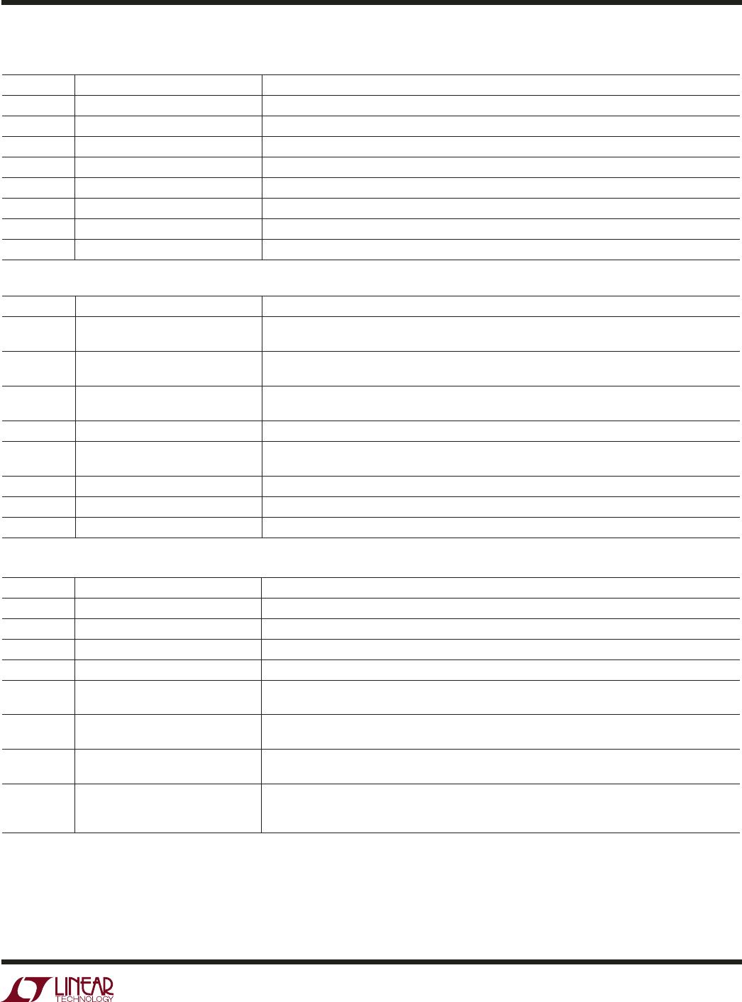
Table 11. FAULT1 Register E (04h) – Read/Write
BIT NAME OPERATION
E7 –12V Overcurrent Fault Occurred Indicates Overcurrent Fault Occurred on –12V Supply
1 = Overcurrent Fault Occurred, 0 = No Overcurrent Faults
E6 3.3V Overcurrent Fault Occurred Indicates Overcurrent Fault Occurred on 3.3V Supply
1 = Overcurrent Fault Occurred, 0 = No Overcurrent Faults
E5 5V Overcurrent Fault Occurred Indicates Overcurrent Fault Occurred on 5V Supply
1 = Overcurrent Fault Occurred, 0 = No Overcurrent Faults
E4 12V Overcurrent Fault Occurred Indicates Overcurrent Fault Occurred on 12V Supply
1 = Overcurrent Fault Occurred, 0 = No Overcurrent Faults
E3 –12V Undervoltage Fault Occurred Indicates –12V Supply Undervoltage Fault Occurred When V
EEIN
Went High
1 = V
EEIN
was High, 0 = No Undervoltage Faults
E2 3.3V Undervoltage Fault Occurred Indicates 3.3V Supply Undervoltage Fault Occurred When 3V
IN
Went Low
1 = 3V
IN
was Low, 0 = No Undervoltage Faults
E1 5V Undervoltage Fault Occurred Indicates 5V Supply Undervoltage Fault Occurred When 5V
IN
Went Low
1 = 5V
IN
was Low, 0 = No Undervoltage Faults
E0 12V Undervoltage Fault Occurred Indicates 12V Supply Undervoltage Fault Occurred When 12V
IN
Went Low
1 = 12V
IN
was Low, 0 = No Undervoltage Faults
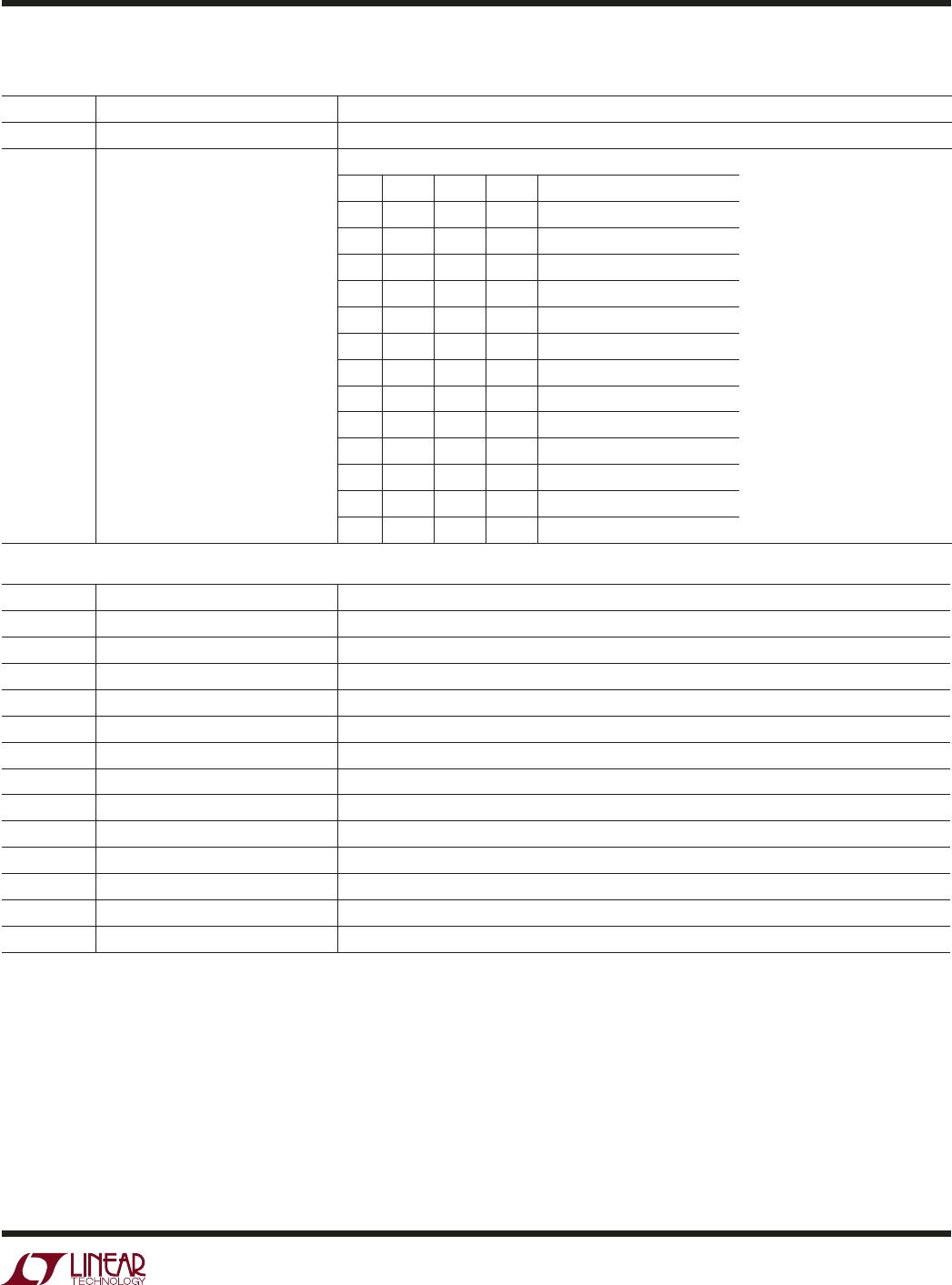
Table 12. FAULT2 Register F (05h) – Read/Write
BIT NAME OPERATION
F7 GPIO1 Changed State Indicates that GPIO1 Pin Changed State; 1 = GPIO1 Changed State, 0 = GPIO1 Unchanged
F6 BD_SEL# Changed State Indicates that BD_SEL# Pin Changed State; 1 = BD_SEL# Changed State, 0 = BD_SEL# Unchanged
F5 FET Short Fault Occurred Indicates Potential FET Short was Detected on at Least One Supply, When ADC Measured Current
Sense Voltage Exceeded 7 LSB While FET was Off; 1 = FET was Shorted, 0 = FET is Good
F4 PGI Fault Occurred Indicates PGI Fault Occurred; 1 = PGI Fault Occurred, 0 = No PGI faults
F3 –12V Power Bad Fault Occurred Indicates –12V Power was Bad When V
EEOUT
Went High
1 = V
EEOUT
was High, 0 = No Power Bad Faults
F2 3.3V Power Bad Fault Occurred Indicates 3.3V Power was Bad When 3V
OUT
Went Low
1 = 3V
OUT
was Low, 0 = No Power Bad Faults
F1 5V Power Bad Fault Occurred Indicates 5V Power was Bad When 5V
OUT
Went Low
1 = 5V
OUT
was Low, 0 = No Power Bad Faults
F0 12V Power Bad Fault Occurred Indicates 12V Power was Bad When 12V
OUT
Went Low
1 = 12V
OUT
was Low, 0 = No Power Bad Faults
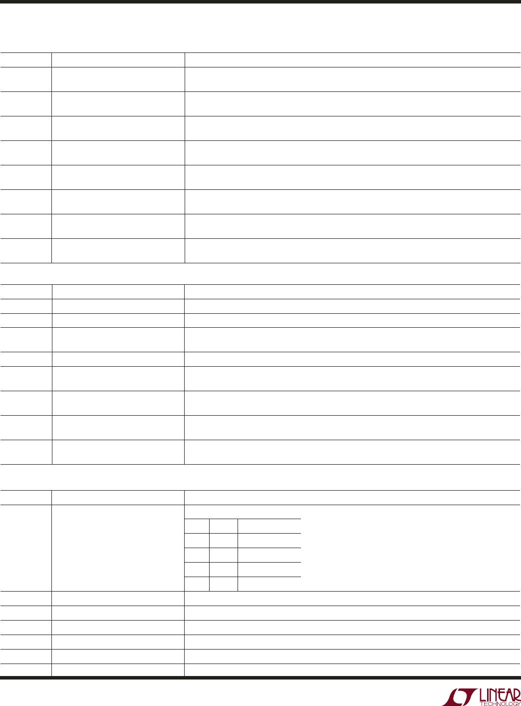
Table 13. GPIO Register G (06h) – Read/Write (GPIO2, GPIO3 Bits Apply Only to the UHF Package)
BIT NAME OPERATION
G7:6 GPIO Select Control Which GPIO Pin is Multiplexed to the GPIO Channel of ADC
G7 G6 GPIO
0 0 GPIO1 (Default)
0 1 GPIO1
1 0 GPIO2
1 1 GPIO3
G5 GPIO3 Output GPIO3 Pin Open-Drain Output State; 1 = High Impedance (Default), 0 = Pulls Low
G4 GPIO2 Output GPIO2 Pin Open-Drain Output State; 1 = High Impedance (Default), 0 = Pulls Low
G3 GPIO1 Output GPIO1 Pin Open-Drain Output State; 1 = High Impedance (Default), 0 = Pulls Low
G2 GPIO3 Input State of the GPIO3 Pin, Read Only Bit; 1 = GPIO3 High, 0 = GPIO3 Low
G1 GPIO2 Input State of the GPIO2 Pin, Read Only Bit; 1 = GPIO2 High, 0 = GPIO2 Low
G0 GPIO1 Input State of the GPIO1 Pin, Read Only Bit; 1 = GPIO1 High, 0 = GPIO1 Low
APPLICATIO S I FOR ATIO
WUU
U