LTC4245
16
4245fa
When a switch is to be turned on, an internal 100μA cur-
rent source is connected to the TIMER pin and a 20μA
current to SS pin. The gate of each ramping supply’s pass
transistor is servoed by an internal amplifi er, so the supply
current never exceeds an internal current limit. This internal
current limit starts off with a negative value, which makes
the amplifi er pull the gate low. The voltage ramp on the
SS pin is converted to a current limit rising linearly with
time. The amplifi er releases the gate as the current limit
crosses zero. An internal current source starts charging
up the gate. When the gate voltage reaches the MOSFET
threshold voltage, the switch begins to turn on. The
amplifi er once again starts modulating the gate pull-up
current so that the sense resistor voltage drop follows the
internally set current limit. The rate of rise of the inrush
current is given by:
dI
dt
G
R
dV
dt
INRUSH SS
SENSE
SS
=
(1)
dV
dt
I
C
SS SS
SS
=
(2)
G
SS
is the ratio of the change in current limit to the change
in SS pin voltage. The rising current limit will stop at a
level depending on the foldback circuit. The foldback circuit
monitors the outputs of all supplies which are ramping.
In the worst case, a supply output could be shorted to
ground. In this case the foldback circuit reduces the cur-
rent limit to 30% of the maximum as shown in the Typical
Performance Curves. To set an inrush current lower than
the foldback level, a series R-C network can be connected
between the gate pin and ground (V
EEOUT
for –12V supply)
(Figure 3). This allows charging the output load beyond
the time dictated by the TIMER capacitor. When the rising
internal current limit exceeds the dV/dt set inrush current,
the current limit amplifi er goes open loop. If any ramping
supply’s amplifi er is open loop the SS pin current drops
to 2μA from 20μA, thus slowing the current limit rise.
This would affect the other supplies ramp-up in case of
simultaneous turn-on. A 100kΩ resistance ensures that
the capacitor charge is decoupled during a fast gate turn-
off. The capacitor value is determined by:
C
I
I
C
GATE
GATE UP
INRUSH
LOAD
=
()
(3)
Meanwhile the TIMER pin ramps up to 2.56V, when it is
reset to ground. Current limit faults on the ramping supplies
are ignored during this time period. The start-up timing
cycle ends when the TIMER pin falls below 0.23V. The SS
pin is reset, the circuit breaker for the supply is armed and
its current limit raised to 3x the circuit breaker threshold.
In a sequenced turn-on the part will start another TIMER
and SS cycle to ramp up the next supply. If supplies are
being turned on through the serial bus, it will wait for the
next turn-on command.
Once all supplies have been turned on and all their outputs
are within tolerance, HEALTHY# will pull low and LO-
CAL_PCI_RST#, which was low, will now follow PCI_RST#.
The TIMER pin is now pulled up by a 10μA current source
while SS pin remains in reset. When TIMER reaches 2.56V,
it is reset to ground. As it crosses 0.23V the PGI pin is
sampled. If it is low then all switches are turned off.
APPLICATIO S I FOR ATIO
WUU
U
TIME 50ms/DIV
SS
2.5V/DIV
TIMER
2.5V/DIV
4245 F02
12V
OUT
, 5V
OUT
3V
OUT
, V
EEOUT
, 10V/DIV
BD_SEL#
5V/DIV
HEALTHY#
5V/DIV
LOCAL_PCI_RST#
5V/DIV
Figure 2. Normal Turn-On Waveform
Figure 3. C
GATE
for dV/dt Limited Inrush Current
34
1817
4245 F03
R26
100k
R6
10
R8
10
Q2, Si7880DP
V
EEGATE
5V
GATE
C
GATE(5V)
LTC4245G*
V
EEOUT
Q4, Si4872
R27
100k
C
GATE(VEE)
*ADDITIONAL DETAILS
OMITTED FOR CLARITY
LTC4245
17
4245fa
Turn-Off
The switches can be turned off by a variety of condi-
tions.
1. ON pin going low or BD_SEL# going high turns off all
switches.
2. Individual switches can be turned off by resetting
the particular FET On control bit (D0 to D3) through
the serial bus.
3. A variety of fault conditions will turn off all switches
together. These include supply undervoltage,
overcurrent circuit breaker and PGI faults.
4. Writing a logic one into the undervoltage, overcurrent
or PGI fault bits will turn off all switches, if the
corresponding autoretry is not enabled.
Normally the 12V, 5V and 3.3V switches are turned off
with a 1.3mA current pulling down the gate to ground.
V
EEGATE
is pulled through a resistive switch to V
EEIN
. All
supply outputs are also discharged to ground through
internal switches. When any MOSFET is shut off, the
HEALTHY# signal pulls high and LOCAL_PCI_RST# will
be asserted low. Figure 4 shows all supplies being turned
off by BD_SEL# going high.
ON Register and Sequencing
The LTC4245 features an ON register (Table 10) consisting
of four On control bits (D0 to D3) and four On status bits
(D4 to D7). D0 to D3 provide independent on/off control
for each supply through the I
2
C bus. Bits D4 to D7 report
the on status of each supply. Even though a supply may
be commanded to turn-on by setting its On control bit,
it may remain off (On status bit low) because the condi-
tions to turn on, as listed in the Turn-On section, may not
be present.
The sequence control bit, C6, determines whether the four
supply MOSFETs turn-on together or in a fi xed sequence.
The default state is no sequencing. In this case taking
the ON pin high sets all the four On control bits. If the
start-up conditions are satisfi ed, all switches will turn on
under the control of a single TIMER and SS cycle. Due to
different input voltage offsets in the current limit amplifi er
of each supply, the gate turn-on of all MOSFETs will not
occur at the same moment but will happen in random
order depending on amplifi er offset and soft-start ramp
rate. The gate turn-ons will be truly simultaneous only if
SS pin is left open.
If bit C6 is set, then the ON pin going high sets only the
12V On control bit, D0. The 12V back-end supply ramps
up. The end of the TIMER and SS cycle sets the 5V On
control bit, D1, starting the ramp of the 5V supply output.
The end of the 5V timing cycle sets bit D2 and the end of
the 3.3V ramp sets bit D3. In this way, the four On control
APPLICATIO S I FOR ATIO
WUU
U
Figure 4. Normal Turn-Off Waveform
TIME 100ms/DIV
4245 F04
12V
OUT
, 5V
OUT
3V
OUT
, V
EEOUT
, 10V/DIV
BD_SEL#
5V/DIV
HEALTHY#
5V/DIV
LOCAL_PCI_RST#
5V/DIV
Figure 5. Sequential Turn-On Waveform
TIME 50ms/DIV
4245 F05
SS
2.5V/DIV
TIMER
2.5V/DIV
12V
OUT
, 5V
OUT
3V
OUT
, V
EEOUT
, 10V/DIV
BD_SEL#
5V/DIV
HEALTHY#
5V/DIV
LOCAL_PCI_RST#
5V/DIV
bits get set one after another, leading to a 12V, 5V, 3.3V,
–12V start-up sequence. Figure 5 illustrates this. If C6 is set
and any of the start-up conditions goes bad, all switches
turn-off, and all On control bits except D0 are reset. This
ensures that the part goes through a sequenced turn-on
during auto-retry. D1 to D3 are also reset when BD_SEL#
goes low with C6 set.
LTC4245
18
4245fa
When the sequence bit C6 is set, setting the On control
bit of a supply, through the I
2
C interface, starts the supply
turn-on sequence from that supply onwards. For example,
setting bit D1 will turn-on 5V, 3.3V, –12V supplies, in that
order. A logic one can then be written to bit D0 to ramp
the 12V supply. At the end of this ramp-up, bit D1 is set.
But since 5V is already powered-up, the sequence stops
there.
The I
2
C interface provides the most fl exibility in turning
supplies on and off. With bit C6 cleared, any supply or
supplies can be turned on by setting their On control
bits. The On control bits cannot be set when any supply
is ramping (therefore using TIMER and SS pins). The SS
busy bit, A1, indicates this blanking period. The On control
bits can be reset though, even when a supply is ramping.
Two or more On control bits may be set at the same time
to ramp multiple supplies in the same timing cycle. When
all supplies are turned on the LTC4245 goes through the
PGI timing cycle.
Supply Voltage Confi guration
The CFG pin enables the LTC4245 to be used in non-CPCI
applications. It is a three-state input pin. In a CPCI applica-
tion with all four supplies, the CFG pin is tied to ground.
Floating the CFG pin disables the V
EE
undervoltage lockout
(UVLO), start-up foldback and power bad functions. It also
makes the ±12V turn-ons coincident by using the 12V FET
On control bit, D0, to control the –12V supply MOSFET.
This allows the three positive supplies to power-up and
HEALTHY# to assert, even when a negative supply is
either unavailable or does not meet the required thresh-
olds. If unused the V
EEIN
, V
EESENSE
, V
EEGATE
and V
EEOUT
pins should be tied to ground. Since the circuit breaker
and active current limit circuits are not disabled, a lower
negative supply could be hot plugged. It would turn on
whenever the 12V supply turns on. Care should be taken
that the supply does not collapse under overcurrent con-
ditions. At low supplies, the ECB and ACL circuits stop
functioning. With the UVLO already disabled, the LTC4245
may not detect a fault condition on the V
EE
supply. Large
currents, limited only by MOSFET and sense resistances,
could fl ow, potentially damaging the board traces and
connector pins.
If the CFG pin is tied high, the 5V supply thresholds change
to 3.3V levels, while keeping the fl oating state functionality.
The 5V supply UVLO, power bad thresholds and foldback
profi le become similar to those of the 3.3V supply. The
5V
IN
and 5V
OUT
inputs to the ADC use the same LSB and
full-scale as the 3V
IN
and 3V
OUT
pins. This allows the use
of an extra 3.3V supply instead of a 5V supply as in a PCI
Express application.
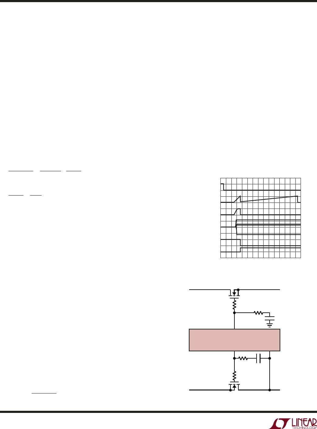
Overcurrent Fault
The LTC4245 has different current limiting behavior dur-
ing start-up, when supply ramps up under TIMER and SS
control, and normal operation. As such it can generate an
overcurrent fault during both phases of operation. Both
set the faulting supply’s overcurrent fault bit (bits E4 to
E7) and shut off all external FETs.
During start-up when both TIMER and SS are ramping,
the current limit is a function of SS pin voltage and the
ramping supplies’ output voltages. A supply could power
up entirely in current limit depending on the bypass ca-
pacitor at the outputs of the ramping supplies. The TIMER
pin sets the time duration for current limit during start-up.
This time involves the TIMER charging up to 2.56V with a
100μA current source and then resetting to 0.23V with a
switch. At the end of the timing cycle if the supply is still
in current limit, i.e., the gate of it’s external MOSFET is still
being actively controlled, an overcurrent fault is declared
for that supply and all MOSFETs are shut off (Figure 6).
Therefore the maximum time a supply can stay in current
limit at start-up is given by:
tCK C msF
START T TMCAP T
==
••./23 3 µ
(4)
APPLICATIO S I FOR ATIO
WUU
U
Figure 6. Start-Up Into a Short on 3.3V Output
TIME 10ms/DIV
4245 F06
3.3V SUPPLY
CURRENT 2.5A/DIV
3V
GATE
2.5V/DIV
SS 2.5V/DIV
TIMER 2.5V/DIV
ON 5V/DIV
12V
OUT
, 5V
OUT
3V
OUT
, V
EEOUT
,
10V/DIV
HEALTHY#
5V/DIV

LTC4245IUHF#PBF

Mfr. #:
Manufacturer:
Analog Devices Inc.
Description:
Hot Swap Voltage Controllers Quad Hot Swap Contr. w/ADC and I2C
Lifecycle:
New from this manufacturer.
Delivery:
DHL FedEx Ups TNT EMS
Payment:
T/T Paypal Visa MoneyGram Western Union