LTC2927
7
2927fb
0.8V
–
+
–
+
5
RAMPBUF
5
RAMP
2927 F06
5
V
CC
5
5
FB
5
ON
5
TRACK
1.2V
10μA
10μA
V
CC
1x
R
ONB
R
ONA
MASTER
SLAVE
DC/DC
C
RAMP
R
TB
R
FB
R
FA
R
TA
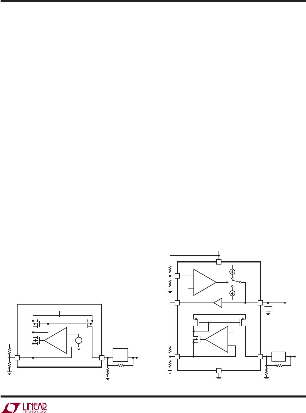
Figure 6. Simplifi ed Functional DiagramFigure 5. Simplifi ed Tracking Cell
0.8V
–
+
2927 F05
5
FB
5
TRACK
V
CC
MASTER
SLAVE
FB OUT
DC/DC
R
TB
R
FB
R
FA
R
TA
+
–
pin is mirrored at the FB pin to establish a voltage at the
output of the slave supply. The slave output voltage varies
with the master signal, enabling the slave supply to be
controlled as a function of the master signal with terms
set by R
TA
and R
TB
. By selecting appropriate values of
R
TA
and R
TB
, it is possible to generate any of the profi les
in Figures 1 to 4.
Controlling the Ramp-Up and Ramp-Down Behavior
The operation of the LTC2927 is most easily understood
by referring to the simplifi ed functional diagram in Figure
6. When the ON pin is low, the master signal at the RAMP
pin is pulled to ground. Since the current through R
TB
is
at its maximum when the master signal is low, the current
from FB is also at its maximum. This current drives the
slave output to its minimum voltage.
When the ON pin rises above 1.23V, the master signal
rises and the slave supply tracks the master signal. The
ramp rate is set by an external capacitor driven by a 10μA
current source at the RAMP pin. Alternatively, the RAMP
pin can be connected to a separate supply to be used as
the master signal.
In a properly designed system, when the master signal
has reached its maximum voltage the current from the
TRACK pin is zero. In this case, there is no current from
the FB pin and the LTC2927 has no effect on the output
voltage accuracy, transient response or stability of the
slave supply.
When the ON pin falls below V
ON(TH)
– ΔV
ON(HYST)
, typi-
cally 1.225V, the RAMP pin pulls down with 10μA and the
master signal and slave supplies will fall at the same rate
as they rose previously.
The ON pin can be controlled by a digital I/O pin or it
can be used to monitor an input supply. By connecting a
resistive divider from an input supply to the ON pin, the
supplies will ramp up only after the monitored supply has
reached a preset voltage.
If a resistive divider is used to set the ON pin voltage, choose
values that will keep this voltage above the maximum ON
pin threshold voltage of 1.25V at the lowest operating
supply level.
The Ramp Buffer
The RAMPBUF pin provides a buffered version of the
RAMP pin voltage that drives the resistive divider on the
TRACK pin. The buffered master signal provides up to
2mA to drive the resistors.
Shutdown Output
In some applications it might be necessary to control
the shutdown or RUN/SS pins of the slave supplies. The
LTC2927 may not be able to supply the rated 1mA of current
from the FB pin when V
CC
is below 2.9V. If the slave power
supply is capable of operating at low input voltages, use
the open-drain SDO output to drive the SHDN or RUN/SS
pin of the slave supply (see Figure 7). This will hold the
slave supply output low until the ON pin is above 1.23V
and V
CC
is above the 2.5V undervoltage lockout condition.
APPLICATIO S I FOR ATIO
WUU
U

