MC1496, MC1496B
http://onsemi.com
7
−30
f, FREQUENCY (MHz)
20
10
0
−10
−20
0.1 1.0 10 1000.01
R
L
= 3.9 k
R
e
= 500
R
L
= 3.9 k
R
e
= 2.0 k
|V
C
| = 0.5 Vdc
R
L
= 500
R
e
= 1.0 k
R
L
= 3.9 k (Standard
R
e
= 1.0 k Test Circuit)
A , SINGLE-ENDED VOLTAGE GAIN (dB)
V
S
1001.0
Side Band
0.3
0.4
0
1000
f
C
, CARRIER FREQUENCY (MHz)
0.6
0.9
1.0
10
0.8
0.7
0.1
0.2
0.5
0.1
21, TRANSADMITTANCE (mmho)
80
0
f
C
±3f
S
800600400200
V
S
, INPUT SIGNAL AMPLITUDE (mVrms)
f
C
±2f
S
0
60
50
40
30
20
10
70
SUPPRESSION BELOW EACH FUNDAMENTAL
CARRIER SIDEBAND (dB)
f
C
2f
C
505.00.05 0.1 0.5 1.0 10
3f
C
0
60
50
40
30
20
10
70
f
C
, CARRIER FREQUENCY (MHz)
SUPPRESSION BELOW EACH FUNDAMENTAL
CARRIER SIDEBAND (dB)
T
A
, AMBIENT TEMPERATURE (°C)
MC1496
(70°C)
−75 −50
60
7550250−25
50
40
30
20
10
100 125 150 175
70
CS
V , CARRIER SUPPRESION (dB)
A
V
+
R
L
R
e
) 2r
e
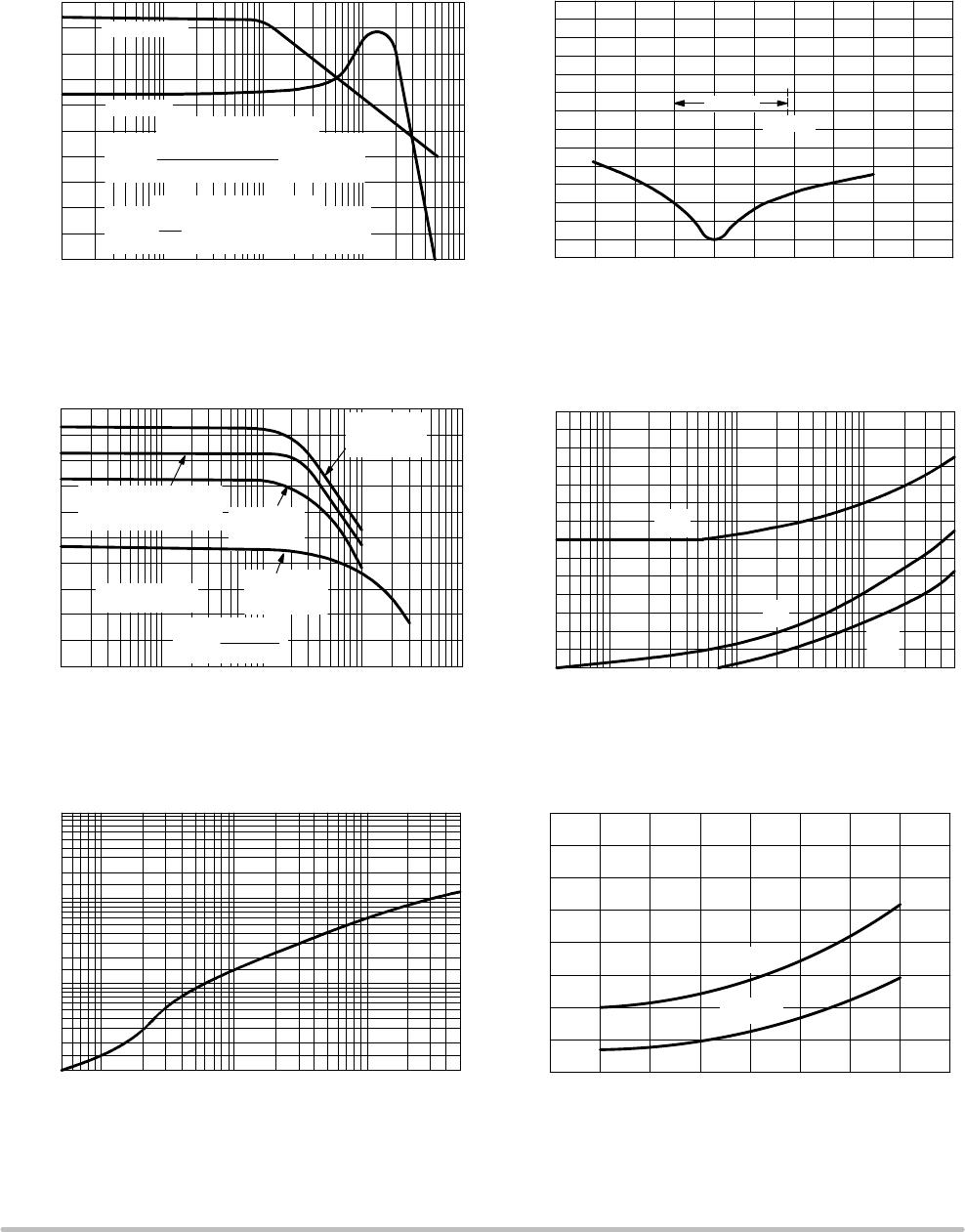
TYPICAL CHARACTERISTICS (continued)
Typical characteristics were obtained with circuit shown in Figure 5, f
C
= 500 kHz (sine wave),
V
C
= 60 mVrms, f
S
= 1.0 kHz, V
S
= 300 mVrms, T
A
= 25°C, unless otherwise noted.
0.1
5010
10
1.0
0.01
1.0 5.00.05 0.1 0.5
f
C
, CARRIER FREQUENCY (MHz)
V , CARRIER OUTPUT VOLTAGE (mVrms)
CFT
Signal Port
0
Figure 15. Sideband and Signal Port
Transadmittances versus Frequency
Figure 16. Carrier Suppression
versus Temperature
Figure 17. SignalPort Frequency Response Figure 18. Carrier Suppression
versus Frequency
Figure 19. Carrier Feedthrough
versus Frequency
Figure 20. Sideband Harmonic Suppression
versus Input Signal Level
γ
21
+
I
out
V
in
V
out
+ 0|V
C
| + 0.5Vdc
21
+
I
out
(EachSideband)
V
in
(Signal)
V
out
+ 0
Sideband Transadmittance
Signal Port Transadmittance
MC1496, MC1496B
http://onsemi.com
8
500100 4003000 200
V
C
, CARRIER INPUT LEVEL (mVrms)
f
C
= 10 MHz
0
60
50
40
30
20
10
70
CS
V , CARRIER SUPPRESSION (dB)
2f
C
±f
S
2f
C
±2f
S
3f
C
±f
S
f
C
, CARRIER FREQUENCY (MHz)
50101.0 5.00.05 0.1 0.5
0
60
50
40
30
20
10
70
SUPPRESSION BELOW EACH FUNDAMENTAL
CARRIER SIDEBAND (dB)
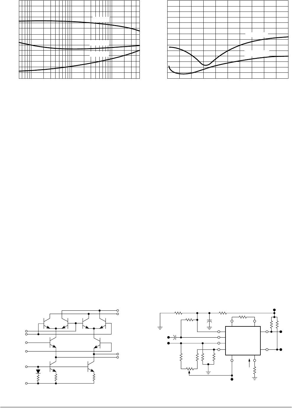
Figure 21. Suppression of Carrier Harmonic
Sidebands versus Carrier Frequency
Figure 22. Carrier Suppression versus
Carrier Input Level
f
C
= 500 kHz
OPERATIONS INFORMATION
The MC1496, a monolithic balanced modulator circuit, is
shown in Figure 23.
This circuit consists of an upper quad differential amplifier
driven by a standard differential amplifier with dual current
sources. The output collectors are crosscoupled so that
fullwave balanced multiplication of the two input voltages
occurs. That is, the output signal is a constant times the
product of the two input signals.
Mathematical analysis of linear ac signal multiplication
indicates that the output spectrum will consist of only the sum
and difference of the two input frequencies. Thus, the device
may be used as a balanced modulator, doubly balanced mixer,
product detector, frequency doubler, and other applications
requiring these particular output signal characteristics.
The lower differential amplifier has its emitters connected
to the package pins so that an external emitter resistance may
be used. Also, external load resistors are employed at the
device output.
Signal Levels
The upper quad differential amplifier may be operated
either in a linear or a saturated mode. The lower differential
amplifier is operated in a linear mode for most applications.
For lowlevel operation at both input ports, the output
signal will contain sum and difference frequency
components and have an amplitude which is a function of the
product of the input signal amplitudes.
For highlevel operation at the carrier input port and
linear operation at the modulating signal port, the output
signal will contain sum and difference frequency
components of the modulating signal frequency and the
fundamental and odd harmonics of the carrier frequency.
The output amplitude will be a constant times the
modulating signal amplitude. Any amplitude variations in
the carrier signal will not appear in the output.
The linear signal handling capabilities of a differential
amplifier are well defined. With no emitter degeneration, the
maximum input voltage for linear operation is
approximately 25 mV peak. Since the upper differential
amplifier has its emitters internally connected, this voltage
applies to the carrier input port for all conditions.
Since the lower differential amplifier has provisions for an
external emitter resistance, its linear signal handling range
may be adjusted by the user. The maximum input voltage for
linear operation may be approximated from the following
expression:
V = (I5) (R
E
) volts peak.
This expression may be used to compute the minimum
value of R
E
for a given input voltage amplitude.
Signal
Input
Carrier
Input
8 (+)
500500 500
14V
EE
Bias
V
C
(Pin numbers
per G package)
V
o
,
Output
(−) 12
2
Gain
Adjust
3
(+) 6
V
S
10 (−)
4 (−)
1 (+)
5
−V
o
R
e
1.0 k
2
12 Vdc
R
L
3.9 k
+V
o
V
EE
−8.0 Vdc
6.8 k
I5
14
0.1 F
12
MC1496
6
8
1.0 k1.0 k
50 k
51
10 k
10 k
0.1 F
Carrier
Input
Modulating
Signal
Input
V
S
V
C
Carrier Null
51
3
51
4
1
10
5
R
L
3.9 k
Figure 23. Circuit Schematic Figure 24. Typical Modulator Circuit
MC1496, MC1496B
http://onsemi.com
9
Table 1. Voltage Gain and Output Frequencies
Carrier Input Signal (V
C
) Approximate Voltage Gain Output Signal Frequency(s)
Lowlevel dc
R
L
V
C
2(R
E
) 2r
e
)
ǒ
KT
q
Ǔ
f
M
Highlevel dc
R
L
R
E
) 2r
e
f
M
Lowlevel ac
R
L
V
C
(rms)
22
Ǹ
ǒ
KT
q
Ǔ
(R
E
) 2r
e
)
f
C
±f
M
Highlevel ac
0.637 R
L
R
E
) 2r
e
f
C
±f
M
, 3f
C
±f
M
, 5f
C
±f
M
, . . .
2. Lowlevel Modulating Signal, V
M
, assumed in all cases. V
C
is Carrier Input Voltage.
3. When the output signal contains multiple frequencies, the gain expression given is for the output amplitude ofeach of the two desired outputs,
f
C
+ f
M
and f
C
f
M
.
4. All gain expressions are for a singleended output. For a differential output connection, multiply each expression by two.
5. R
L
= Load resistance.
6. R
E
= Emitter resistance between Pins 2 and 3.
7. r
e
= Transistor dynamic emitter resistance, at 25°C;
re [
26 mV
I
5
(mA)
8. K = Boltzmanns Constant, T = temperature in degrees Kelvin, q = the charge on an electron.
The gain from the modulating signal input port to the
output is the MC1496 gain parameter which is most often of
interest to the designer. This gain has significance only when
the lower differential amplifier is operated in a linear mode,
but this includes most applications of the device.
As previously mentioned, the upper quad differential
amplifier may be operated either in a linear or a saturated
mode. Approximate gain expressions have been developed
for the MC1496 for a lowlevel modulating signal input and
the following carrier input conditions:
1) Lowlevel dc
2) Highlevel dc
3) Lowlevel ac
4) Highlevel ac
These gains are summarized in Table 1, along with the
frequency components contained in the output signal.
APPLICATIONS INFORMATION
Double sideband suppressed carrier modulation is the
basic application of the MC1496. The suggested circuit for
this application is shown on the front page of this data sheet.
In some applications, it may be necessary to operate the
MC1496 with a single dc supply voltage instead of dual
supplies. Figure 25 shows a balanced modulator designed
for operation with a single 12 Vdc supply. Performance of
this circuit is similar to that of the dual supply modulator.
AM Modulator
The circuit shown in Figure 26 may be used as an
amplitude modulator with a minor modification.
All that is required to shift from suppressed carrier to AM
operation is to adjust the carrier null potentiometer for the
proper amount of carrier insertion in the output signal.
However, the suppressed carrier null circuitry as shown in
Figure 26 does not have sufficient adjustment range.
Therefore, the modulator may be modified for AM
operation by changing two resistor values in the null circuit
as shown in Figure 27.
Product Detector
The MC1496 makes an excellent SSB product detector
(see Figure 28).
This product detector has a sensitivity of 3.0 V and a
dynamic range of 90 dB when operating at an intermediate
frequency of 9.0 MHz.
The detector is broadband for the entire high frequency
range. For operation at very low intermediate frequencies
down to 50 kHz the 0.1 F capacitors on Pins 8 and 10 should
be increased to 1.0 F. Also, the output filter at Pin 12 can
be tailored to a specific intermediate frequency and audio
amplifier input impedance.
As in all applications of the MC1496, the emitter
resistance between Pins 2 and 3 may be increased or
decreased to adjust circuit gain, sensitivity, and dynamic
range.
This circuit may also be used as an AM detector by
introducing carrier signal at the carrier input and an AM
signal at the SSB input.
The carrier signal may be derived from the intermediate
frequency signal or generated locally. The carrier signal may
MC1496DR2G

Mfr. #:
Manufacturer:
ON Semiconductor
Description:
Modulator / Demodulator Balanced Mod/DeMod
Lifecycle:
New from this manufacturer.
Delivery:
DHL FedEx Ups TNT EMS
Payment:
T/T Paypal Visa MoneyGram Western Union