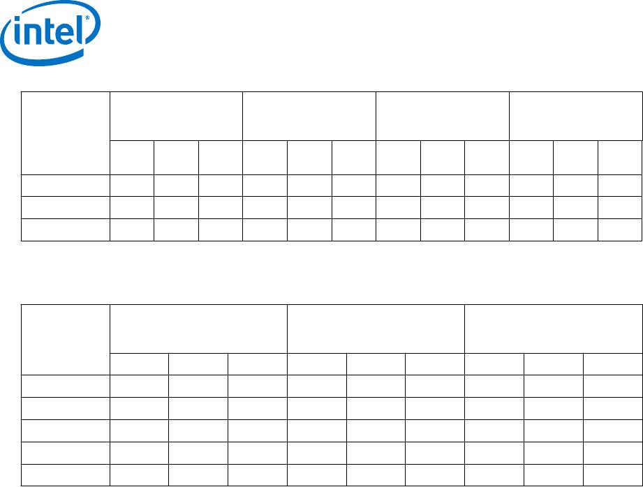
I/O Vertical Migration for Intel Arria 10 Devices
Figure 4. Migration Capability Across Intel Arria 10 Product Lines
• The arrows indicate the migration paths. The devices included in each vertical migration path are shaded.
Devices with fewer resources in the same path have lighter shades.
• To achieve the full I/O migration across product lines in the same migration path, restrict I/Os and
transceivers usage to match the product line with the lowest I/O and transceiver counts.
• An LVDS I/O bank in the source device may be mapped to a 3 V I/O bank in the target device. To use
memory interface clock frequency higher than 533 MHz, assign external memory interface pins only to
banks that are LVDS I/O in both devices.
• There may be nominal 0.15 mm package height difference between some product lines in the same
package type.
• Some migration paths are not shown in the Intel Quartus Prime software Pin Migration View.
Variant
Product
Line
Package
U19 F27 F29 F34 F35 KF40 NF40 RF40 NF45 SF45 UF45
Intel® Arria® 10 GX
GX 160
GX 220
GX 270
GX 320
GX 480
GX 570
GX 660
GX 900
GX 1150
Intel Arria 10 GT
GT 900
GT 1150
Intel Arria 10 SX
SX 160
SX 220
SX 270
SX 320
SX 480
SX 570
SX 660
Note: To verify the pin migration compatibility, use the Pin Migration View window in the
Intel Quartus Prime software Pin Planner.
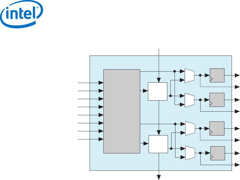
Adaptive Logic Module
Intel Arria 10 devices use a 20 nm ALM as the basic building block of the logic fabric.
The ALM architecture is the same as the previous generation FPGAs, allowing for
efficient implementation of logic functions and easy conversion of IP between the
device generations.
The ALM, as shown in following figure, uses an 8-input fracturable look-up table (LUT)
with four dedicated registers to help improve timing closure in register-rich designs
and achieve an even higher design packing capability than the traditional two-register
per LUT architecture.
Intel
®
Arria
®
10 Device Overview
A10-OVERVIEW | 2018.04.09
Intel
®
Arria
®
10 Device Overview
17