LM75A_4 © NXP B.V. 2007. All rights reserved.
Product data sheet Rev. 04 — 10 July 2007 4 of 24
NXP Semiconductors
LM75A
Digital temperature sensor and thermal watchdog
7. Functional description
7.1 General operation
The LM75A uses the on-chip band gap sensor to measure the device temperature with
the resolution of 0.125 °C and stores the 11-bit 2's complement digital data, resulted from
11-bit A-to-D conversion, into the device Temp register. This Temp register can be read at
any time by a controller on the I
2
C-bus. Reading temperature data does not affect the
conversion in progress during the read operation.
The device can be set to operate in either mode: normal or shutdown. In normal operation
mode, the temp-to-digital conversion is executed every 100 ms and the Temp register is
updated at the end of each conversion. In shutdown mode, the device becomes idle, data
conversion is disabled and the Temp register holds the latest result; however, the device
I
2
C-bus interface is still active and register write/read operation can be performed. The
device operation mode is controllable by programming bit B0 of the configuration register.
The temperature conversion is initiated when the device is powered-up or put back into
normal mode from shutdown.
In addition, at the end of each conversion in normal mode, the temperature data (or Temp)
in the Temp register is automatically compared with the overtemperature shutdown
threshold data (or Tos) stored in the Tos register, and the hysteresis data (or Thyst) stored
in the Thyst register, in order to set the state of the device OS output accordingly. The
device Tos and Thyst registers are write/read capable, and both operate with 9-bit
2's complement digital data. To match with this 9-bit operation, the Temp register uses
only the 9 MSB bits of its 11-bit data for the comparison.
The way that the OS output responds to the comparison operation depends upon the OS
operation mode selected by configuration bit B1, and the user-defined fault queue defined
by configuration bits B3 and B4.
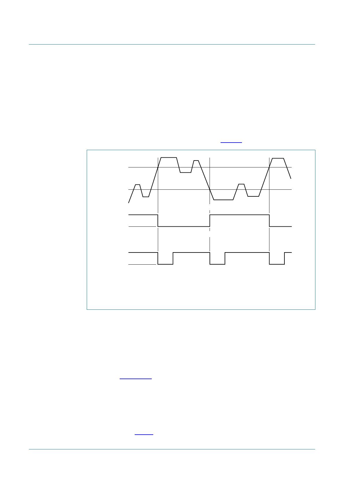
In OS comparator mode, the OS output behaves like a thermostat. It becomes active
when the Temp exceeds the T
os
, and is reset when the Temp drops below the T
hyst
.
Reading the device registers or putting the device into shutdown does not change the
state of the OS output. The OS output in this case can be used to control cooling fans or
thermal switches.
In OS interrupt mode, the OS output is used for thermal interruption. When the device is
powered-up, the OS output is first activated only when the Temp exceeds the T
os
; then it
remains active indefinitely until being reset by a read of any register. Once the OS output
has been activated by crossing T
os
and then reset, it can be activated again only when the
Temp drops below the T
hyst
; then again, it remains active indefinitely until being reset by a
read of any register. The OS interrupt operation would be continued in this sequence:
T
os
trip, Reset, T
hyst
trip, Reset, T
os
trip, Reset, T
hyst
trip, Reset, etc.
A1 6 Digital input. User-defined address bit 1.
A0 7 Digital input. User-defined address bit 0.
V
CC
8 Power supply.
Table 3. Pin description
…continued
Symbol Pin Description
LM75A_4 © NXP B.V. 2007. All rights reserved.
Product data sheet Rev. 04 — 10 July 2007 5 of 24
NXP Semiconductors
LM75A
Digital temperature sensor and thermal watchdog
In both cases, comparator mode and interrupt mode, the OS output is activated only if a
number of consecutive faults, defined by the device fault queue, has been met. The fault
queue is programmable and stored in the two bits, B3 and B4, of the Configuration
register. Also, the OS output active state is selectable as HIGH or LOW by setting
accordingly the configuration register bit B2.
At power-up, the device is put into normal operation mode, the T
os
is set to 80 °C, the T
hyst
is set to 75 °C, the OS active state is selected LOW and the fault queue is equal to 1. The
temp reading data is not available until the first conversion is completed in about 100 ms.
The OS response to the temperature is illustrated in Figure 4.
7.2 I
2
C-bus serial interface
The LM75A can be connected to a compatible 2-wire serial interface I
2
C-bus as a slave
device under the control of a controller or master device, using two device terminals, SCL
and SDA. The controller must provide the SCL clock signal and write/read data to/from the
device through the SDA terminal. Notice that if the I
2
C-bus common pull-up resistors have
not been installed as required for I
2
C-bus, then an external pull-up resistor, about 10 k,
is needed for each of these two terminals. The bus communication protocols are
described in Section 7.10.
7.3 Slave address
The LM75A slave address on the I
2
C-bus is partially defined by the logic applied to the
device address pins A2, A1 and A0. Each of them is typically connected either to GND for
logic 0, or to V
CC
for logic 1. These pins represent the three LSB bits of the device 7-bit
address. The other four MSB bits of the address data are preset to ‘1001’ by hard wiring
inside the LM75A. Table 4 shows the device’s complete address and indicates that up to
(1) OS is reset by either reading register. It is assumed that the fault queue is met at each T
os
and
T
hyst
crossing point.
Fig 4. OS response to temperature
002aad032
(1) (1) (1)
T
os
T
hyst
OS reset
OS active
OS reset
OS active
OS output in comparator mode
OS output in interrupt mode
reading temperature limits
LM75A_4 © NXP B.V. 2007. All rights reserved.
Product data sheet Rev. 04 — 10 July 2007 6 of 24
NXP Semiconductors
LM75A
Digital temperature sensor and thermal watchdog
8 devices can be connected to the same bus without address conflict. Because the input
pins, SCL, SDA and A2 to A0, are not internally biased, it is important that they should not
be left floating in any application.
7.4 Register list
The LM75A contains four data registers beside the pointer register as listed in Table 5.
The pointer value, read/write capability and default content at power-up of the registers
are also shown in Table 5.
7.4.1 Pointer register
The Pointer register contains an 8-bit data byte, of which the two LSB bits represent the
pointer value of the other four registers, and the other 6 MSB bits are equal to 0, as shown
in Table 6 and Table 7. The Pointer register is not accessible to the user, but is used to
select the data register for write/read operation by including the pointer data byte in the
bus command.
Because the Pointer value is latched into the Pointer register when the bus command
(which includes the pointer byte) is executed, a read from the LM75A may or may not
include the pointer byte in the statement. To read again a register that has been recently
read and the pointer has been preset, the pointer byte does not have to be included. To
Table 4. Address table
1 = HIGH; 0 = LOW.
MSB LSB
1001A2A1A0
Table 5. Register table
Register
name
Pointer
value
R/W POR
state
Description
Conf 01h R/W 00h Configuration register: contains a single 8-bit data
byte; to set the device operating condition; default = 0.
Temp 00h read only n/a Temperature register: contains two 8-bit data bytes;
to store the measured Temp data.
Tos 03h R/W 5000h Overtemperature shutdown threshold register:
contains two 8-bit data bytes; to store the
overtemperature shutdown T
os
limit; default = 80 °C.
Thyst 02h R/W 4B00h Hysteresis register: contains two 8-bit data bytes;
to store the hysteresis T
hyst
limit; default = 75 °C.
Table 6. Pointer register
B7 B6 B5 B4 B3 B2 B[1:0]
0 0 0 0 0 0 pointer value
Table 7. Pointer value
B1 B0 Selected register
0 0 Temperature register (Temp)
0 1 Configuration register (Conf)
1 0 Hysteresis register (Thyst)
1 1 Overtemperature shutdown register (Tos)

LM75AD,118

Mfr. #:
Manufacturer:
NXP Semiconductors
Description:
Board Mount Temperature Sensors I2C LOCAL +/- 2OC TS
Lifecycle:
New from this manufacturer.
Delivery:
DHL FedEx Ups TNT EMS
Payment:
T/T Paypal Visa MoneyGram Western Union