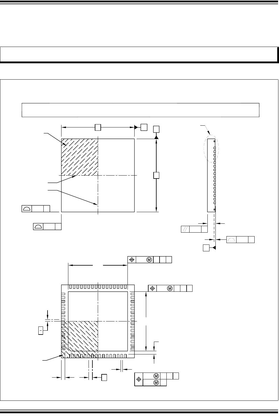
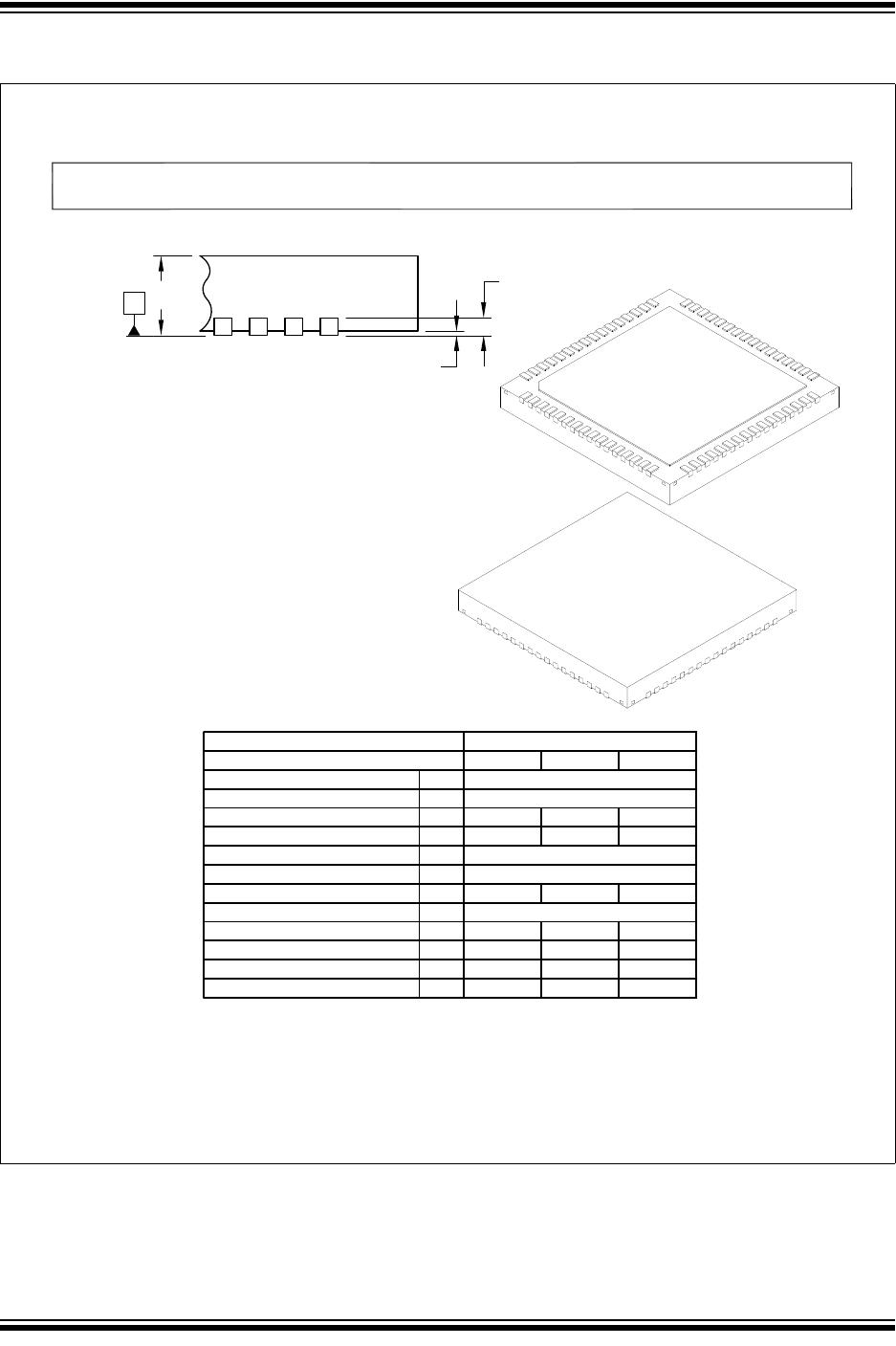
RECOMMENDED LAND PATTERN
Dimension Limits
Units
C2
Optional Center Pad Width
Contact Pad Spacing
Optional Center Pad Length
Contact Pitch
Y2
X2
6.60
6.60
MILLIMETERS
0.40 BSC
MIN
E
MAX
7.90
Contact Pad Length (X64)
Contact Pad Width (X64)
Y1
X1
0.80
0.20
Microchip Technology Drawing C04-2437A
NOM
64-Lead Very Thin Plastic Quad Flat, No Lead Package (JXX) - 8x8 mm Body [VQFN]
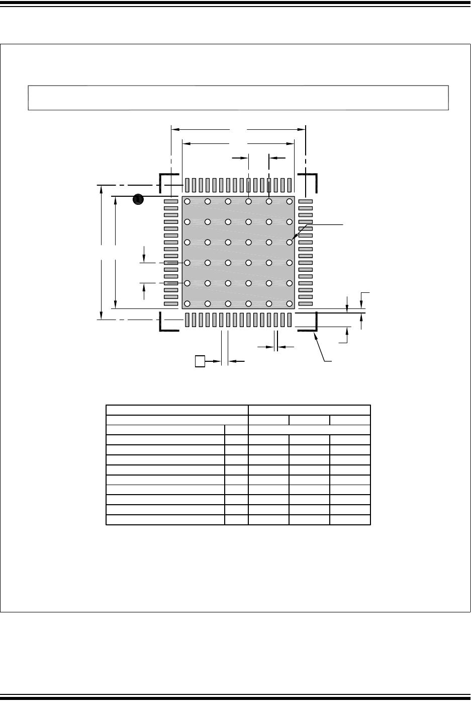
SILK SCREEN
1
2
64
C1
C2
E
X1
Y1
G1
Y2
X2
C1Contact Pad Spacing 7.90
Contact Pad to Center Pad (X64) G1 0.20
Thermal Via Diameter V
Thermal Via Pitch EV
0.33
1.20
ØV
EV
EV
BSC: Basic Dimension. Theoretically exact value shown without tolerances.
Notes:
Dimensioning and tolerancing per ASME Y14.5M
For best soldering results, thermal vias, if used, should be filled or tented to avoid solder loss during
reflow process
1.
2.
For the most current package drawings, please see the Microchip Packaging Specification located at
http://www.microchip.com/packaging
Note: