IP4220CZ6 All information provided in this document is subject to legal disclaimers. © NXP B.V. 2011. All rights reserved.
Product data sheet Rev. 5 — 8 July 2011 3 of 9
NXP Semiconductors
IP4220CZ6
Dual USB 2.0 integrated ESD protection
7. Characteristics
[1] Pins 1, 3, 4 and 6.
[2] Pins 1, 3, 4 and 6 to ground.
[3] Pin 5 to pin 2.
8. Application information
8.1 Universal serial bus 2.0 protection
The device is optimized to protect, for example, two USB 2.0 ports from ESD. Each device
can protect both USB data lines and the V
BUS
supply line. A typical application is shown in
Figure 1
.
Table 6. Characteristics
T
amb
=25
C; unless otherwise specified.
Symbol Parameter Conditions Min Typ Max Unit
C
(I/O-GND)
input/output to
ground capacitance
V
I
=0V; f=1MHz;
V
P
=3V
[1]
-1.0-pF
C
(zd-GND)
Zener diode to
ground capacitance
V
I
=0V; f=1MHz;
V
P
=3V
[3]
-40-pF
I
RM
reverse leakage current V
I
=3V
[2]
- - 100 nA
V
BRzd
Zener diode breakdown
voltage
I=1mA
[3]
6- 9V
V
F
forward voltage - 0.7 - V
Fig 1. Typical application of IP4220CZ6
IP4220CZ6 All information provided in this document is subject to legal disclaimers. © NXP B.V. 2011. All rights reserved.
Product data sheet Rev. 5 — 8 July 2011 4 of 9
NXP Semiconductors
IP4220CZ6
Dual USB 2.0 integrated ESD protection
9. Package outline
Fig 2. Package outline SOT457 (SC-74)
REFERENCES
OUTLINE
VERSION
EUROPEAN
PROJECTION
ISSUE DATE
IEC JEDEC JEITA
SOT457 SC-74
wBM
b
p
D
e
pin 1
index
A
A
1
L
p
Q
detail X
H
E
E
v M
A
AB
y
scale
c
X
132
4
56
0 1 2 mm
Plastic surface-mounted package (TSOP6); 6 leads SOT457
UNIT
A
1
b
p
cD
E
H
E
L
p
Qywv
mm
0.1
0.013
0.40
0.25
3.1
2.7
0.26
0.10
1.7
1.3
e
0.95
3.0
2.5
0.2 0.10.2
DIMENSIONS (mm are the original dimensions)
0.6
0.2
0.33
0.23
A
1.1
0.9
05-11-07
06-03-16
IP4220CZ6 All information provided in this document is subject to legal disclaimers. © NXP B.V. 2011. All rights reserved.
Product data sheet Rev. 5 — 8 July 2011 5 of 9
NXP Semiconductors
IP4220CZ6
Dual USB 2.0 integrated ESD protection
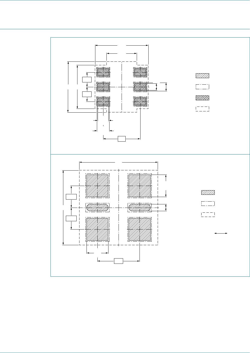
10. Soldering
Fig 3. Reflow soldering footprint SOT457 (SC-74)
Fig 4. Wave soldering footprint SOT457 (SC-74)
solder lands
solder resist
occupied area
solder paste
sot457_fr
3.45
1.95
2.8253.3
0.45
(6×)
0.55
(6×)
0.7
(6×)
0.8
(6×)
2.4
0.95
0.95
Dimensions in mm
sot457_fw
5.3
5.05
1.45
(6×)
0.45
(2×)
1.5
(4×)
2.85
1.475
1.475
solder lands
solder resist
occupied area
preferred transport
direction during soldering
Dimensions in mm

IP4220CZ6F

Mfr. #:
Manufacturer:
Nexperia
Description:
TVS Diodes / ESD Suppressors IP4220CZ6/SC-74/REEL 13" Q1/T1
Lifecycle:
New from this manufacturer.
Delivery:
DHL FedEx Ups TNT EMS
Payment:
T/T Paypal Visa MoneyGram Western Union

Products related to this Datasheet