DS1904
7 of 13
The idle state for the 1-Wire bus is high. If for any reason a transaction needs to be suspended, the bus
m
ust be left in the idle state if the transaction is to resume. If this does not occur and the bus is left low
for more than 120 µs, one or more of the devices on the bus may be reset. Since the DS1904 gets all its
energy for operation through its V
DD
pin it will not perform a power-on reset if the 1-Wire bus is low for
an extended time period.
Transaction Sequence
The protocol for accessing the DS1904 via the 1-Wire port is as follows:
Initialization
ROM Function Command
Clock Function Command
INITIALIZATION
All transactions on the 1-Wire bus begin with an initialization sequence. The initialization sequence con-
s
ists of a reset pulse transmitted by the bus master followed by presence pulse(s) transmitted by the
slave(s). The presence pulse lets the bus master know that the DS1904 is on the bus and is ready to
operate. For more details, see the 1-Wire Signaling section.
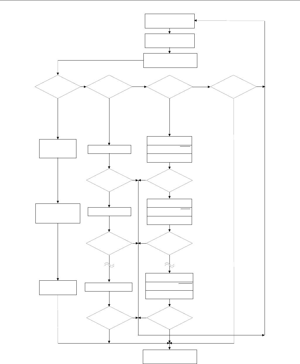
ROM FUNCTION COMMANDS
Once the bus master has detected a presence, it can issue one of the four ROM function commands that
the DS1904 supports. All ROM function commands are eight bits long. A list of these commands follows
(refer to flowchart in Figure 7):
Read ROM [33h]
This command allows the bus master to read the DS1904’s 8-bit family code, unique 48-bit serial num-
ber, and 8-bit CRC. This command should only be used if there is a single slave on the bus. If more than
one slave is present on the bus, a data collision will occur when all slaves try to transmit at the same time
(open drain will produce a wired-AND result). The resultant family code and 48-bit serial number read by
the master will be invalid.
Match ROM [55h]
The match ROM command, followed by a 64-bit ROM sequence, allows the bus master to address a spe-
c
ific DS1904 on a multidrop bus. Only the DS1904 that exactly matches the 64-bit ROM sequence will
respond to the following clock function command. All slaves that do not match the 64-bit ROM sequence
will wait for a reset pulse. This command can be used with a single or multiple devices on the bus.
SEARCH ROM [F0h]
When a system is initially brought up, the bus master might not know the number of devices on the
1-Wire bus or their 64-bit ROM codes. The search ROM command allows the bus master to use a process
of elimination to identify the 64-bit ROM codes of all slave devices on the bus. The search ROM process
is the repetition of a simple 3-step routine: read a bit, read the complement of the bit, then write the de-
sired value of that bit. The bus master performs this 3-step routine on each bit of the ROM. After one
complete pass, the bus master knows the 64-bit ROM code of one device. Additional passes will identify
the ROM codes of the remaining devices. See Chapter 5 of the Book of i
Button® Standards for a
comprehensive discussion of a search ROM, including an actual example.
DS1904
8 of 13
ROM FUNCTIONS FLOW CHART F
igure 7
F0H
Search ROM
Command
?
DS1904 TX Bit 0
DS1904 TX Bit 0
Master TX Bit 0
Bit 0
Match ?
DS1904 TX Bit 1
DS1904 TX Bit 1
Master TX Bit 1
Bit 1
Match ?
DS1904 TX Bit 63
DS1904 TX Bit 63
Master TX Bit 63
Bit 63
Match ?
Master TX Control
Function Command
33H
Read ROM
Command
?
DS1904 TX
Serial Number
6 Bytes
DS1904 TX
CRC Byte
DS1904 TX
Family Code
1 Byte
Match ROM
55H
Command
?
Bit 0
Match ?
Bit 1
Match ?
Bit 63
Match ?
Master TX Bit 1
Master TX Bit 0
N
Y
N
Y
N N
Y
N N
N N
Y
Y
Y
Y
Y
Y
(SEE FIGURE 5)
Master TX ROM
Function Command
Master TX
Reset Pulse
DS1904 TX
Presence Pulse
CCH
Skip ROM
Command
?
N
Y
N
Master TX Bit 63
DS1904
9 of 13
Skip ROM [CCh]
This command can save time in a single drop bus system by allowing the bus master to access the clock
f
unctions without providing the 64-bit ROM code. If more than one slave is present on the bus and, for
example, a read command is issued following the Skip ROM command, data collision will occur on the
bus as multiple slaves transmit simultaneously (open drain pull-downs will produce a wired-AND result).
1–WIRE SIGNALING
The DS1904 requires strict protocols to ensure data integrity. The protocol consists of four types of sig-
naling on one line: Reset Sequence with Reset Pulse and Presence Pulse, Write 0, Write 1 and Read Data.
Except for the presence pulse the bus master initiates all these signals.
The initialization sequence required to begin any communication with the DS1904 is shown in Figure 8.
A reset pulse followed by a presence pulse indicates the DS1904 is ready to send or receive data. The bus
master transmits (TX) a reset pulse (t
RSTL
, minimum 480 µs
). The bus master then releases the line and
goes into receive mode (RX). The 1-Wire bus is pulled to a high state via the pull-up resistor. After
detecting the rising edge on the data line, the DS1904 waits (t
PDH
, 15-60 µs) and then transmits the
presence pulse (t
PDL
, 60-240 µs).
INITIALIZATION PROCEDURE “RESET AND PRESENCE PULSES” Figure 8
RESISTOR
MASTER
DS1904
MASTER RX "PRESENCE PULSE"
480 µs
t
RSTL
<
*
480 µs
t
RSTH
<
**
15 µs
t
PDH
< 60 µs
60
t
PDL
< 240 µs
MASTER TX
"RESET PULSE"
V
PULLUP
V
PULLUP MIN
V
IH MIN
V
IL MAX
0V
t
RSTH
t
RSTL
t
PDH
t
PDL
t
R
* In order not to mask interrupt signaling by other devices on the 1-Wire bus t
RSTL
+ t
R
should al-
ways be less than 960 µs.
** Includes recovery time
READ/WRITE TIME SLOTS
The definitions of write and read time slots are illustrated in Figure 9. The master initiates all time slots
by driving the data line low. The falling edge of the data line synchronizes the DS1904 to the master by
triggering an internal delay circuit. During write time slots, the delay circuit determines when the DS1904
will sample the data line. For a read data time slot, if a “0” is to be transmitted, the delay circuit deter-
mines how long the DS1904 will hold the data line low. If the data bit is a “1”, the DS1904 will not hold
the data line low at all.

DS1904L-F5#

Mfr. #:
Manufacturer:
Maxim Integrated
Description:
iButtons & Accessories RTC iButton
Lifecycle:
New from this manufacturer.
Delivery:
DHL FedEx Ups TNT EMS
Payment:
T/T Paypal Visa MoneyGram Western Union

Products related to this Datasheet