LP2950, LP2951, NCV2951
www.onsemi.com
4
ELECTRICAL CHARACTERISTICS
(V
in
= V
O
+ 1.0 V, I
O
= 100 mA, C
O
= 1.0 mF, T
A
= 25°C [Note 3], unless otherwise noted.)
Characteristic
Symbol Min Typ Max Unit
Output Voltage, 5.0 V Versions V
O
V
V
in
= 6.0 V, I
O
= 100 mA, T
A
= 25°C
LP2950C−5.0/LP2951C/NCV2951C* 4.950 5.000 5.050
LP2950AC−5.0/LP2951AC/NCV2951AC* 4.975 5.000 5.025
T
A
= −40 to +125°C
LP2950C−5.0/LP2951C/NCV2951C* 4.900 5.100
LP2950AC−5.0/LP2951AC/NCV2951AC* 4.940 5.060
V
in
= 6.0 to 30 V, I
O
= 100 mA to 100 mA, T
A
= −40 to +125°C
LP2950C−5.0/LP2951C/NCV2951C* 4.880 5.120
LP2950AC−5.0/LP2951AC/NCV2951AC* 4.925 5.075
Output Voltage, 3.3 V Versions V
O
V
V
in
= 4.3 V, I
O
= 100 mA, T
A
= 25°C
LP2950C−3.3/LP2951C−3.3 3.267 3.300 3.333
LP2950AC−3.3/LP2951AC−3.3/NCV2951AC−3.3* 3.284 3.300 3.317
T
A
= −40 to +125°C
LP2950C−3.3/LP2951C−3.3 3.234 3.366
LP2950AC−3.3/LP2951AC−3.3/NCV2951AC−3.3* 3.260 3.340
V
in
= 4.3 to 30 V, I
O
= 100 mA to 100 mA, T
A
= −40 to +125°C
LP2950C−3.3/LP2951C−3.3 3.221 3.379
LP2950AC−3.3/LP2951AC−3.3/NCV2951AC−3.3* 3.254 3.346
Output Voltage, 3.0 V Versions V
O
V
V
in
= 4.0 V, I
O
= 100 mA, T
A
= 25°C
LP2950C−3.0/LP2951C−3.0 2.970 3.000 3.030
LP2950AC−3.0/LP2951AC−3.0 2.985 3.000 3.015
T
A
= −40 to +125°C
LP2950C−3.0/LP2951C−3.0 2.940 3.060
LP2950AC−3.0/LP2951AC−3.0 2.964 3.036
V
in
= 4.0 to 30 V, I
O
= 100 mA to 100 mA, T
A
= −40 to +125°C
LP2950C−3.0/LP2951C−3.0 2.928 3.072
LP2950AC−3.0/LP2951AC−3.0 2.958 3.042
Product parametric performance is indicated in the Electrical Characteristics for the listed test conditions, unless otherwise noted. Product
performance may not be indicated by the Electrical Characteristics if operated under different conditions.
1. The Junction−to−Ambient Thermal Resistance is determined by PCB copper area per Figure 29.
2. This device series contains ESD protection and exceeds the following tests:
Human Body Model (HBM), 2000 V, Class 2, JESD22 A114−C
Machine Model (MM), 200 V, Class B, JESD22 A115−A
Charged Device Model (CDM), 2000 V, Class IV, JESD22 C101−C
3. Low duty pulse techniques are used during test to maintain junction temperature as close to ambient as possible.
4. V
O(nom)
is the part number voltage option.
5. Noise tests on the LP2951 are made with a 0.01 mF capacitor connected across Pins 7 and 1.
6. Latch−up Current Maximum Rating tested per JEDEC standard: JESD78
− Inputs Low: passing positive current 100 mA and negative current −100 mA
− Inputs High: passing positive current 100 mA and negative current −10 mA.
*NCV prefix is for automotive and other applications requiring site and change control.
LP2950, LP2951, NCV2951
www.onsemi.com
5
ELECTRICAL CHARACTERISTICS (continued)
(V
in
= V
O
+ 1.0 V, I
O
= 100 mA, C
O
= 1.0 mF, T
A
= 25°C [Note 9], unless otherwise noted.)
Characteristic
Symbol Min Typ Max Unit
Line Regulation (V
in
= V
O(nom)
+1.0 V to 30 V) (Note 10) Reg
line
%
LP2950C−XX/LP2951C/LP2951C−XX/NCV2951C* 0.08 0.20
LP2950AC−XX/LP2951AC/LP2951AC−XX/NCV2951AC* 0.04 0.10
Load Regulation (I
O
= 100 mA to 100 mA)
Reg
load
%
LP2950C−XX/LP2951C/LP2951C−XX/NCV2951C* 0.13 0.20
LP2950AC−XX/LP2951AC/LP2951AC−XX/NCV2951AC* 0.05 0.10
Dropout Voltage V
I
− V
O
mV
I
O
= 100 mA
30 80
I
O
= 100 mA 350 450
Supply Bias Current I
CC
I
O
= 100 mA
93 120
mA
I
O
= 100 mA 4.0 12 mA
Dropout Supply Bias Current (V
in
= V
O(nom)
− 0.5 V,
I
O
= 100 mA) (Note 10)
I
CCdropout
110 170
mA
Current Limit (V
O
Shorted to Ground) I
Limit
220 300 mA
Thermal Regulation Reg
thermal
0.05 0.20 %/W
Output Noise Voltage (10 Hz to 100 kHz) (Note 11) V
n
mVrms
C
L
= 1.0 mF
126
C
L
= 100 mF
56
LP2951A/LP2951AC Only
Reference Voltage (T
A
= 25°C) V
ref
V
LP2951C/LP2951C−XX/NCV2951C* 1.210 1.235 1.260
LP2951AC/LP2951AC−XX/NCV2951AC* 1.220 1.235 1.250
Reference Voltage (T
A
= −40 to +125°C) V
ref
V
LP2951C/LP2951C−XX/NCV2951C* 1.200 1.270
LP2951AC/LP2951AC−XX/NCV2951AC* 1.200 1.260
Reference Voltage (T
A
= −40 to +125°C) V
ref
V
I
O
= 100 mA to 100 mA, V
in
= 23 to 30 V
LP2951C/LP2951C−XX/NCV2951C* 1.185 1.285
LP2951AC/LP2951AC−XX/NCV2951AC* 1.190 1.270
Feedback Pin Bias Current I
FB
15 40 nA
Error Comparator
Output Leakage Current (V
OH
= 30 V) I
lkg
0.01 1.0
mA
Output Low Voltage (V
in
= 4.5 V, I
OL
= 400 mA)
V
OL
150 250 mV
Upper Threshold Voltage (V
in
= 6.0 V) V
thu
40 45 mV
Lower Threshold Voltage (V
in
= 6.0 V) V
thl
60 95 mV
Hysteresis (V
in
= 6.0 V) V
hy
15 mV
Shutdown Input
Input Logic Voltage
V
shtdn
V
Logic “0” (Regulator “On”) 0 0.7
Logic “1” (Regulator “Off”) 2.0 30
Shutdown Pin Input Current I
shtdn
mA
V
shtdn
= 2.4 V 35 50
V
shtdn
= 30 V 450 600
Regulator Output Current in Shutdown Mode I
off
3.0 10
mA
(V
in
= 30 V, V
shtdn
= 2.0 V, V
O
= 0, Pin 6 Connected to Pin 7)
Product parametric performance is indicated in the Electrical Characteristics for the listed test conditions, unless otherwise noted. Product
performance may not be indicated by the Electrical Characteristics if operated under different conditions.
7. The Junction−to−Ambient Thermal Resistance is determined by PCB copper area per Figure 29.
8. ESD data available upon request.
9. Low duty pulse techniques are used during test to maintain junction temperature as close to ambient as possible.
10.V
O(nom)
is the part number voltage option.
11. Noise tests on the LP2951 are made with a 0.01 mF capacitor connected across Pins 7 and 1.
*NCV prefix is for automotive and other applications requiring site and change control.
LP2950, LP2951, NCV2951
www.onsemi.com
6
DEFINITIONS
Dropout Voltage − The input/output voltage differential
at which the regulator output no longer maintains regulation
against further reductions in input voltage. Measured when
the output drops 100 mV below its nominal value (which is
measured at 1.0 V differential), dropout voltage is affected
by junction temperature, load current and minimum input
supply requirements.
Line Regulation − The change in output voltage for a
change in input voltage. The measurement is made under
conditions of low dissipation or by using pulse techniques
such that average chip temperature is not significantly
affected.
Load Regulation − The change in output voltage for a
change in load current at constant chip temperature.
Maximum Power Dissipation − The maximum total
device dissipation for which the regulator will operate
within specifications.
Bias Current − Current which is used to operate the
regulator chip and is not delivered to the load.
Output Noise Voltage − The RMS ac voltage at the
output, with constant load and no input ripple, measured
over a specified frequency range.
Leakage Current − Current drawn through a bipolar
transistor collector−base junction, under a specified
collector voltage, when the transistor is “off”.
Upper Threshold Voltage Voltage applied to the
comparator input terminal, below the reference voltage
which is applied to the other comparator input terminal,
which causes the comparator output to change state from a
logic “0” to “1”.
Lower Threshold Voltage Voltage applied to the
comparator input terminal, below the reference voltage
which is applied to the other comparator input terminal,
which causes the comparator output to change state from a
logic “1” to “0”.
Hysteresis The difference between Lower Threshold
voltage and Upper Threshold voltage.
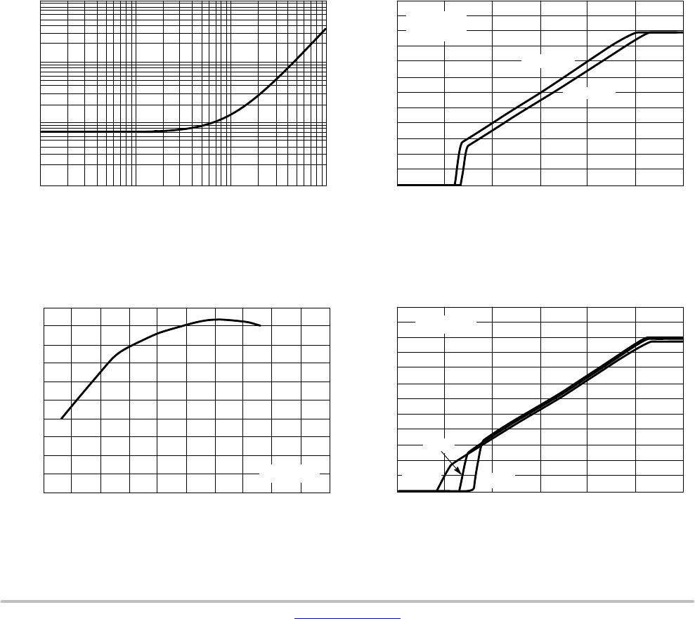
25°C
Figure 2. Quiescent Current
, OUTPUT VOLTAGE (V)
V
out
, OUTPUT VOLTAGE (V)
V
out
-50
5.00
0
6.0
0.1
10
T
A
, AMBIENT TEMPERATURE (°C)
V
in
, INPUT VOLTAGE (V)
LP2950/LP2951 BIAS CURRENT (mA)
I
L
, LOAD CURRENT (mA)
Figure 3. 5.0 V Dropout Characteristics over
Load
Figure 4. Output Voltage versus Temperature
1.0 10 100 1.0 2.0 3.0 4.0 5.0 6.0
0 50 100 150
1.0
0.1
0.01
5.0
4.0
3.0
2.0
1.0
0
4.99
4.98
4.97
4.96
4.95
R
L
= 50 kW
R
L
= 50 W
LP2951C
T
A
= 25°C
LP2951C
200
, OUTPUT VOLTAGE (V)
V
out
0
6.0
V
in
, INPUT VOLTAGE (V)
Figure 5. 5.0 V Dropout Characteristics with
R
L
= 50 W
1.0 2.0 3.0 4.0
5.0
3.0
2.0
1.0
0
6.05.0
4.0
125°C
−40°C
LP2951C

LP2950ACDT-3.0G

Mfr. #:
Manufacturer:
ON Semiconductor
Description:
LDO Voltage Regulators 3V 100mA Low Power
Lifecycle:
New from this manufacturer.
Delivery:
DHL FedEx Ups TNT EMS
Payment:
T/T Paypal Visa MoneyGram Western Union