ICS581-01/02
ZERO DELAY GLITCH-FREE CLOCK MULTIPLEXER ZDB AND MULTIPLEXER
IDT™ / ICS™
ZERO DELAY GLITCH-FREE CLOCK MULTIPLEXER 5
ICS581-01/02 REV L 051310
External Components
The ICS581-01 and ICS581-02 require two 0.01µF capacitors between VDD and GND, one on each side of the
chip. These must be close to the chip to minimize lead inductance. Series termination resistors of 33Ω should be
used on the outputs, should also be close to the chip, and the feedback path should be a direct connection from a
clock output to a FBIN pin, routed directly under the chip to minimize trace length. This should be connected before
the series termination resistor.
Absolute Maximum Ratings
Stresses above the ratings listed below can cause permanent damage to the ICS581-01/02. These ratings, which
are standard values for IDT commercially rated parts, are stress ratings only. Functional operation of the device at
these or any other conditions above those indicated in the operational sections of the specifications is not implied.
Exposure to absolute maximum rating conditions for extended periods can affect product reliability. Electrical
parameters are guaranteed only over the recommended operating temperature range.
Recommended Operation Conditions
DC Electrical Characteristics
Unless stated otherwise, VDD = 3.3 V ±5%, Ambient Temperature -40 to +85° C
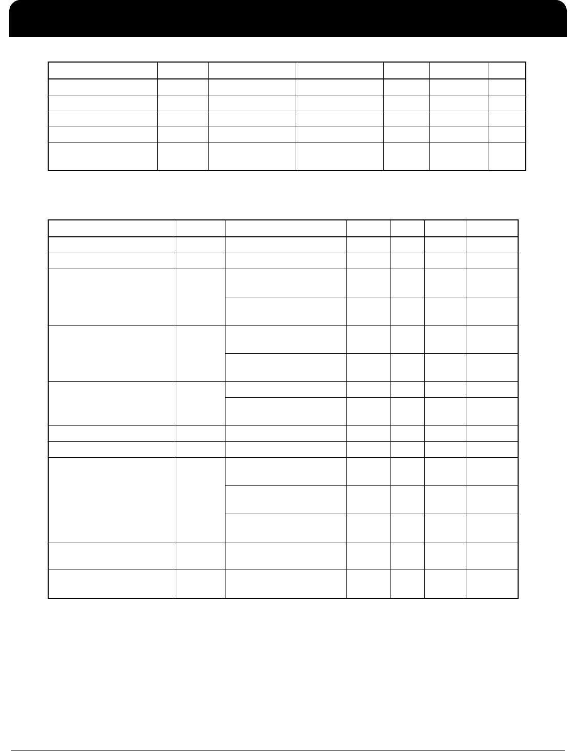
Item Rating
Supply Voltage, VDD 7 V
All Inputs and Outputs -0.5 V to VDD+0.5 V
Ambient Operating Temperature (ICS581-01, ICS581-02) 0 to +70° C
Ambient Operating Temperature (ICS581-01I, ICS581-02I) -40 to +85° C
Storage Temperature -65 to +150° C
Junction Temperature 125° C
Soldering Temperature 260° C
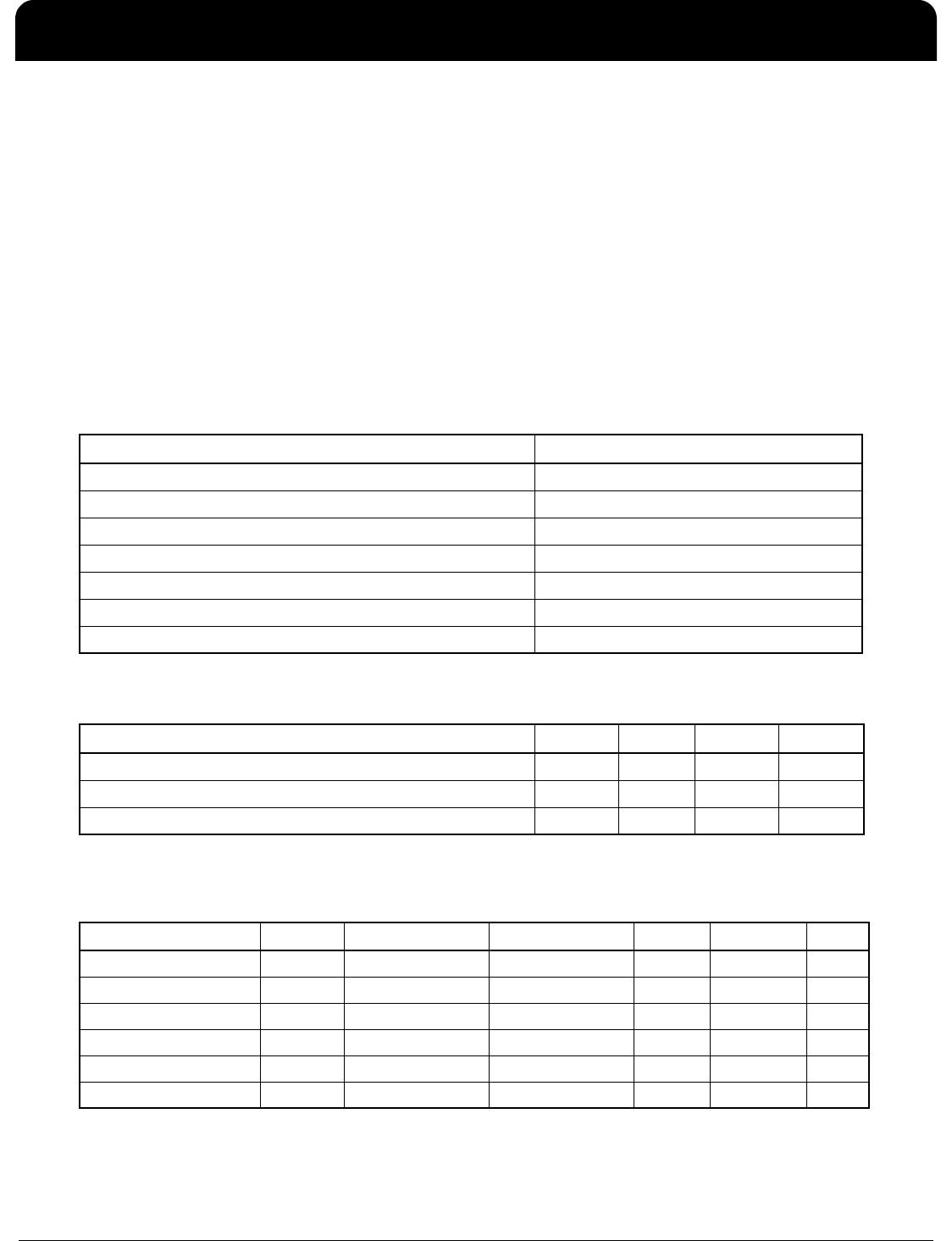
Parameter Min. Typ. Max. Units
Ambient Operating Temperature (ICS581-01, ICS581-02) 0 +70 ° C
Ambient Operating Temperature (ICS581-01I, ICS581-02I) -40 +85 ° C
Power Supply Voltage (measured in respect to GND) +3.0 +5.5 V
Parameter Symbol Conditions Min. Typ. Max. Units
Operating Voltage VDD 3.0 5.5 V
Supply Current IDD 100 MHz, no load 26 mA
Input High Voltage V
IH
Non-clock inputs 2 V
Input Low Voltage V
IL
Non-clock inputs 0.8 V
Input High Voltage V
IH
INA, INB, FBIN (VDD/2)+1 VDD/2 V
Input Low Voltage V
IL
INA, INB, FBIN VDD/2 (VDD/2)-1 V