LTC3588-2
13
35882fc
For more information www.linear.com/LTC3588-2
Figure 7. AC Line Powered 4.1V Li-Ion Battery Charger
35882 F07
PZ1
V
IN
CAP
V
IN2
D0
D1
PZ2
PGOOD
SW
V
OUT
LTC3588-2
DANGER! HIGH VOLTAGE!
GND
150k
Li-Ion
POWER
STREAM
LiR2450
120mAh
22µF
6V
22µH
V
OUT
4.1V
PGOOD
10µF
25V
120VAC
60Hz
F
6V
4.7µF
6V
150k
150k
150k
DANGEROUS AND LETHAL POTENTIALS ARE PRESENT IN OFFLINE CIRCUITS!
BEFORE PROCEEDING ANY FURTHER, THE READER IS WARNED THAT
CAUTION MUST BE USED IN THE CONSTRUCTION, TESTING AND USE OF
OFFLINE CIRCUITS. EXTREME CAUTION MUST BE USED IN WORKING WITH
AND MAKING CONNECTIONS TO THESE CIRCUITS. REPEAT: OFFLINE
CIRCUITS CONTAIN DANGEROUS, AC LINE-CONNECTED HIGH VOLTAGE
POTENTIALS. USE CAUTION. ALL TESTING PERFORMED ON AN OFFLINE
CIRCUIT MUST BE DONE WITH AN ISOLATION TRANSFORMER CONNECTED
BETWEEN THE OFFLINE CIRCUIT’S INPUT AND THE AC LINE. USERS AND
CONSTRUCTORS OF OFFLINE CIRCUITS MUST OBSERVE THIS PRECAUTION
WHEN CONNECTING TEST EQUIPMENT TO THE CIRCUIT TO AVOID ELECTRIC
SHOCK. REPEAT: AN ISOLATION TRANSFORMER MUST BE CONNECTED
BETWEEN THE CIRCUIT INPUT AND THE AC LINE IF ANY TEST EQUIPMENT IS
TO BE CONNECTED.
APPLICATIONS INFORMATION
Figure 8. Electric Field Energy Harvester
35882 F08
PZ1
V
IN
CAP
V
IN2
D1
D0
PZ2
PGOOD
SW
V
OUT
LTC3588-2
GND
10µF
6V
22µH
4.5V
PGOOD
10µF
25V
F
6V
4.7µF
6V
COPPER PANEL
(12" × 24")
COPPER PANEL
(12" × 24")
PANELS ARE PLACED 6"
FROM 2' × 4' FLUORESCENT
LIGHT FIXTURES
Figure 6. Dual Rail Power Supply with Single Piezo
35882 F06
PZ1
V
IN
CAP
V
IN2
D1
D0
PZ2
PGOOD
SW
V
OUT
LTC3588-2
ADVANCED CERAMETRICS
PFCB-W14
GND
10µF
6V
10µF
6V
22µH22µH
3.45V
5.0V
PGOOD2PGOOD1
F
6V
PZ2
V
IN
CAP
V
IN2
D1
D0
PZ1
PGOOD
SW
V
OUT
LTC3588-2
GND
4.7µF
6V
F
6V
4.7µF
6V
10µF
25V
10µF
25V
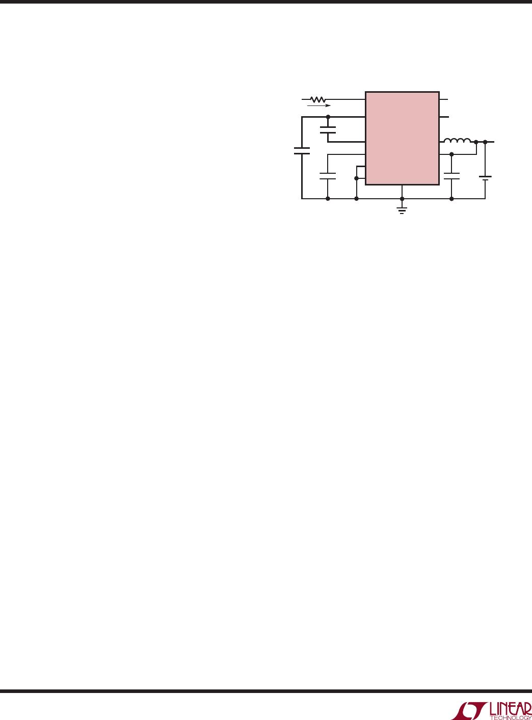
Alternate Power Sources
The LTC3588-2 is not limited to use with piezoelectric ele-
ments but can accommodate a wide variety of input sources
depending on the type of ambient energy available. Figure 7
shows the LTC3588-2 internal bridge rectifier connected
to the AC line in series with four 150k current limiting
resistors. This is a high voltage application and minimum
spacing between the line, neutral, and any high voltage
components should be maintained per the applicable UL
specification. For general off-line applications refer to UL
regulation 1012.
Figure 8 shows an application where copper panels are
placed near a standard fluorescent room light to capacitively
harvest energy from the electric field around the light. The
LTC3588-2
14
35882fc
For more information www.linear.com/LTC3588-2
frequency of the emission will be 120Hz for magnetic bal-
lasts but could be higher if the light uses electronic ballast.
The LTC3588-2 bridge rectifier can handle a wide range
of input frequencies.
Figure 9 shows the LTC3588-2 powered by a 48V com-
munications line. In this example, 1mA is the maximum
current that is allowed to be drawn. The 28k current limiting
resistor sets this current as the LTC3588-2 will shunt V
IN
at 20V. The advantage of this scheme is that the current at
the output is multiplied by the ratio of V
IN
to V
OUT
(less the
loss in the buck converter). This is useful in cases where
greater current is needed at the output than is available
at the input. The high UVLO of 16V prevents any start-up
issue as there is already a good multiplication factor at
APPLICATIONS INFORMATION
Figure 9. Current Fed 3.45V LiFePO
4
Battery Charger
35882 F09
PZ1
V
IN
CAP
V
IN2
D1
D0
PZ2
PGOOD
SW
V
OUT
LTC3588-2
GND
28k
1mA
LiFePO
4
+
22µH
V
OUT
3.45V
3.5mA
PGOOD
47µF
25V
F
6V
48V
4.7µF
6V
10µF
6V
that level. This same technique can be extended to AC
source that also have limited current available at the input.
LTC3588-2
15
35882fc
For more information www.linear.com/LTC3588-2
DD Package
10-Lead Plastic DFN (3mm × 3mm)
(Reference LTC DWG # 05-08-1699 Rev C)
3.00 ±0.10
(4 SIDES)
NOTE:
1. DRAWING TO BE MADE A JEDEC PACKAGE OUTLINE M0-229 VARIATION OF (WEED-2).
CHECK THE LTC WEBSITE DATA SHEET FOR CURRENT STATUS OF VARIATION ASSIGNMENT
2. DRAWING NOT TO SCALE
3. ALL DIMENSIONS ARE IN MILLIMETERS
4. DIMENSIONS OF EXPOSED PAD ON BOTTOM OF PACKAGE DO NOT INCLUDE
MOLD FLASH. MOLD FLASH, IF PRESENT, SHALL NOT EXCEED 0.15mm ON ANY SIDE
5. EXPOSED PAD SHALL BE SOLDER PLATED
6. SHADED AREA IS ONLY A REFERENCE FOR PIN 1 LOCATION ON THE
TOP AND BOTTOM OF PACKAGE
0.40 ± 0.10
BOTTOM VIEW—EXPOSED PAD
1.65 ± 0.10
(2 SIDES)
0.75 ±0.05
R = 0.125
TYP
2.38 ±0.10
(2 SIDES)
15
106
PIN 1
TOP MARK
(SEE NOTE 6)
0.200 REF
0.00 – 0.05
(DD) DFN REV C 0310
0.25 ± 0.05
2.38 ±0.05
(2 SIDES)
RECOMMENDED SOLDER PAD PITCH AND DIMENSIONS
1.65 ±0.05
(2 SIDES)2.15 ±0.05
0.50
BSC
0.70 ±0.05
3.55
±0.05
PACKAGE
OUTLINE
0.25 ± 0.05
0.50 BSC
PIN 1 NOTCH
R = 0.20 OR
0.35 × 45°
CHAMFER
PACKAGE DESCRIPTION
Please refer to http://www.linear.com/designtools/packaging/ for the most recent package drawings.

LTC3588EDD-2#PBF

Mfr. #:
Manufacturer:
Analog Devices / Linear Technology
Description:
Power Management Specialized - PMIC Piezoelectric Energy Harvesting Power Supply
Lifecycle:
New from this manufacturer.
Delivery:
DHL FedEx Ups TNT EMS
Payment:
T/T Paypal Visa MoneyGram Western Union