74HC_HCT4060_Q100 All information provided in this document is subject to legal disclaimers. © NXP B.V. 2013. All rights reserved.
Product data sheet Rev. 2 — 10 April 2013 4 of 25
NXP Semiconductors
74HC4060-Q100; 74HCT4060-Q100
14-stage binary ripple counter with oscillator
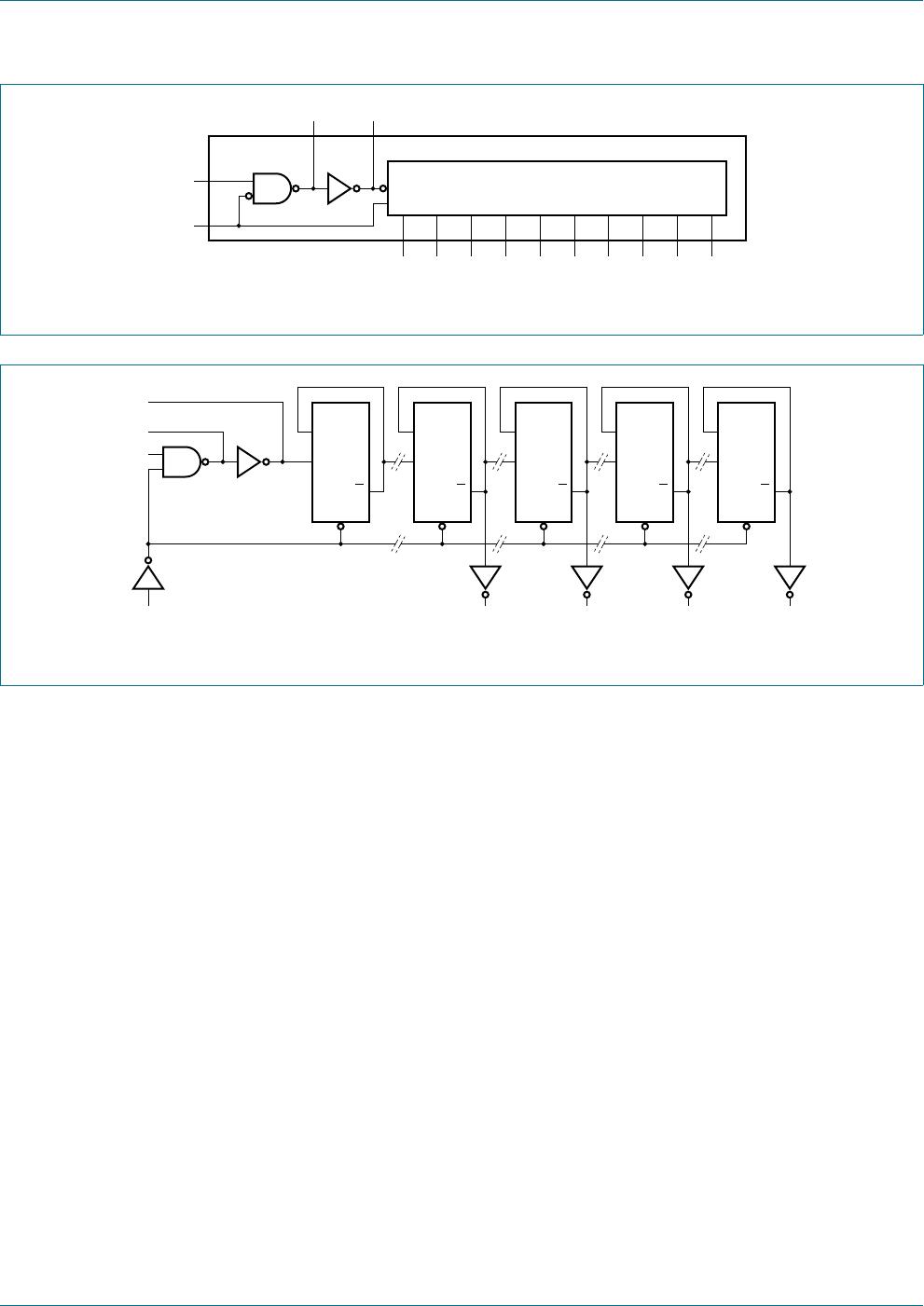
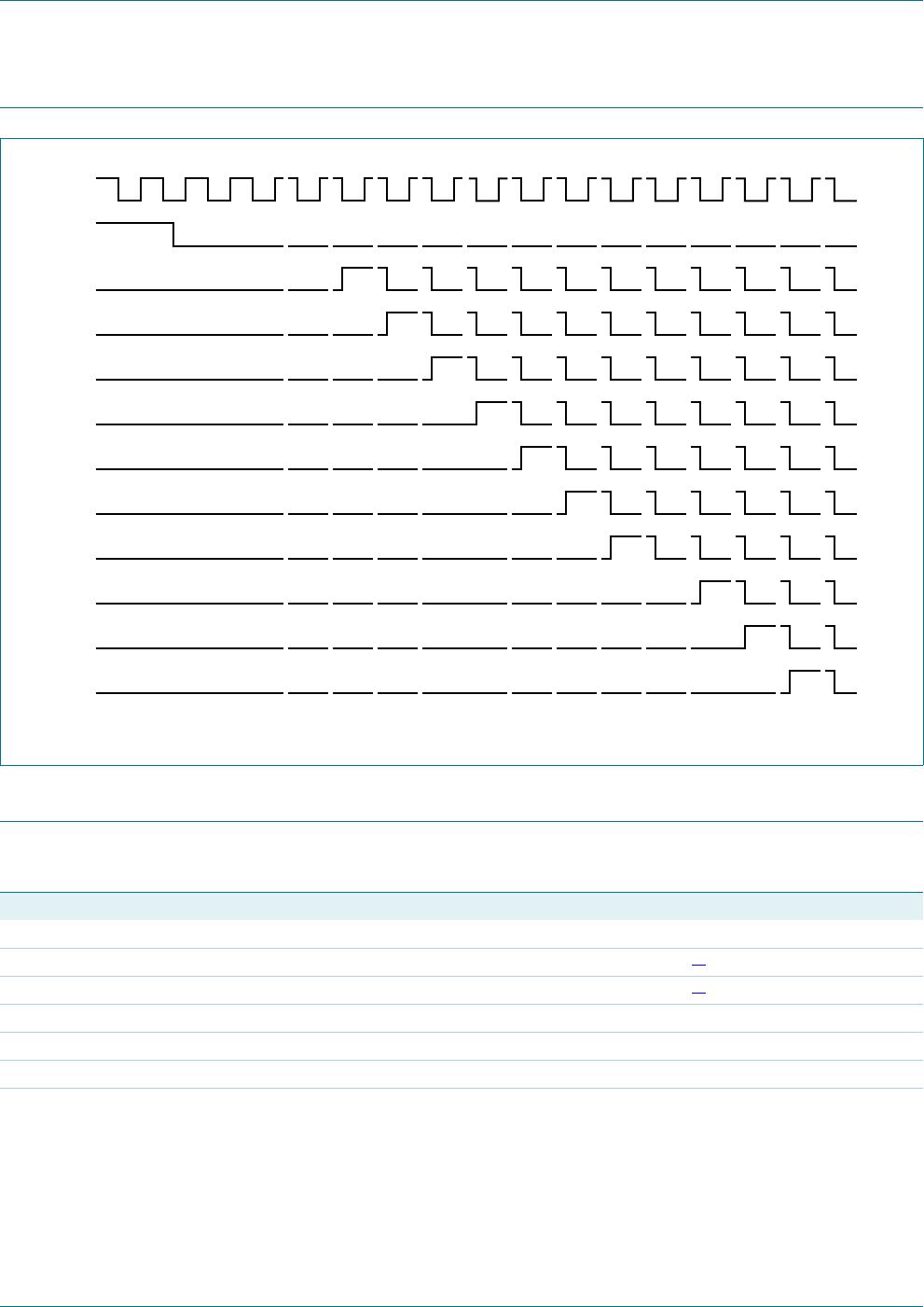
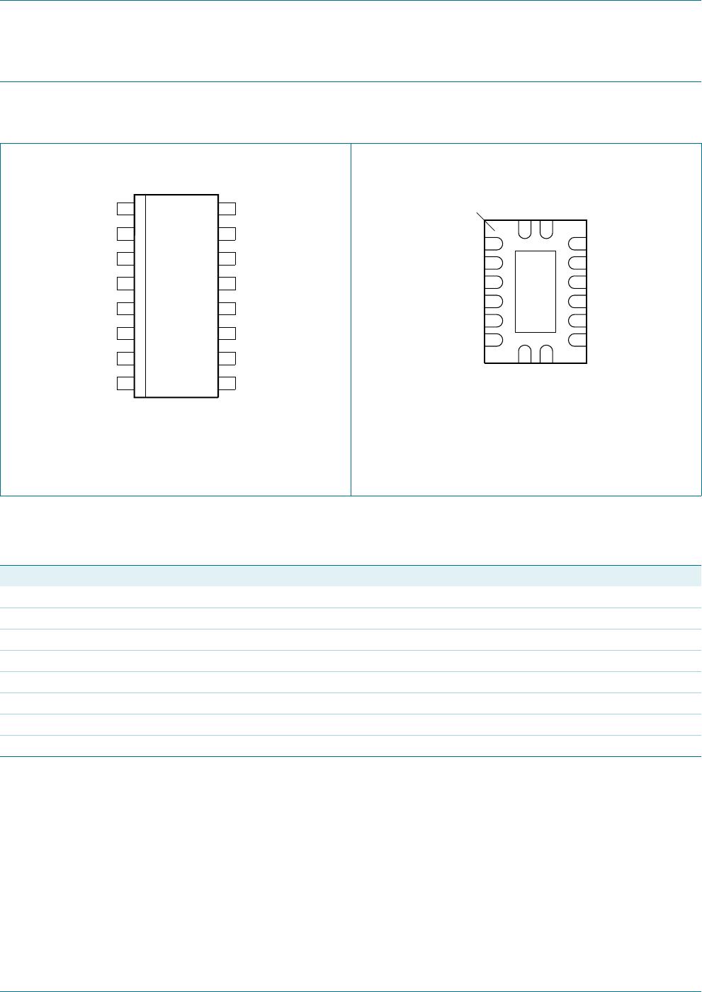
6. Pinning information
6.1 Pinning
6.2 Pin description
(1) The die substrate is attached to this pad using
conductive die attach material. It cannot be used as
supply pin or input.
Fig 5. Pin configuration SO16 and (T)SSOP16 Fig 6. Pin configuration DHVQFN16
+&74
4
4 56
4 05
4 4
4 4
4 4
*1'
&7&
4
9
&&
9
&&
Table 2. Pin description
Symbol Pin Description
Q11 to Q13 1, 2, 3 counter output
Q3 to Q9 7, 5, 4, 6, 14, 13, 15 counter output
GND 8 ground (0 V)
CTC 9 external capacitor connection
RTC 10 external resistor connection
RS 11 clock input /oscillator pin
MR 12 master reset input (active HIGH)
V
CC
16 supply voltage