Expand menu
Hello, Sign in
My Account
0
Cart
Home
Products
Sensors
Semiconductors
Passive Components
Connectors
Power
Electromechanical
Optoelectronics
Circuit Protection
Integrated Circuits - ICs
Main Products
Manufacturers
Blog
Services
About OMO
About Us
Contact Us
Check Stock
NCP1117LPST50T3G
P1-P3
P4-P6
P7-P9
P10-P12
P13-P14
NCP1
1
17LP
www
.onsemi.com
7
TYPICAL CHARACTERISTICS
Figure 22. Line T
ransient Response − V
out
= 2.5 V
Figure 23. Line T
ransient Response − V
out
= 2.5 V
Figure 24. Line T
ransient Response − V
out
= 3.3 V
Figure 25. Line T
ransient Response − V
out
= 3.3 V
−50
0
5.5
4.5
OUTPUT VOL
T
AGE
DEVIA
TION (mV)
INPUT VOL
T
AGE (V)
1 V/
m
s
50
C
in
= 1.0
m
F*
C
out
= 10
m
F*
I
out
= 0.1 A
T
A
= 25
°
C
C
in
= 1.0
m
F*
C
out
= 10
m
F*
I
out
= 0.5 A
T
A
= 25
°
C
−50
0
5.0
4.0
OUTPUT VOL
T
AGE
DEVIA
TION (mV)
INPUT VOL
T
AGE (V)
1 V/
m
s
50
C
in
= 1.0
m
F*
C
out
= 10
m
F*
I
out
= 0.1 A
T
A
= 25
°
C
C
in
= 1.0
m
F*
C
out
= 10
m
F*
I
out
= 0.5 A
T
A
= 25
°
C
*T
antalum Capacitors
*T
antalum Capacitors
*T
antalum Capacitors
*T
antalum Capacitors
Figure 26. Line T
ransient Response − V
out
= 5.0 V
Figure 27. Line T
ransient Response − V
out
= 5.0 V
−50
0
7.5
6.5
OUTPUT VOL
T
AGE
DEVIA
TION (mV)
INPUT VOL
T
AGE (V)
1 V/
m
s
50
C
in
= 1.0
m
F*
C
out
= 10
m
F*
I
out
= 0.1 A
T
A
= 25
°
C
C
in
= 1.0
m
F*
C
out
= 10
m
F*
I
out
= 0.5 A
T
A
= 25
°
C
*T
antalum Capacitors
*T
antalum Capacitors
NCP1
1
17LP
www
.onsemi.com
8
TYPICAL CHARACTERISTICS
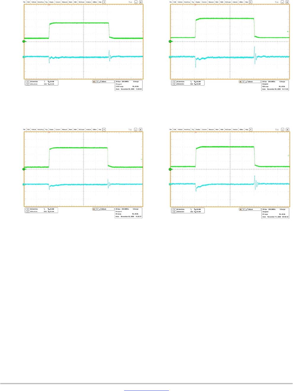
Figure 28. Load T
ransient Response − V
out
= 1.8 V
Figure 29. Load T
ransient Response − V
out
= 2.5 V
C
in
= 10
m
F*
C
out
= 10
m
F*
V
in
= 3.3 V
Preload=0.1A
T
A
= 25
°
C
0
20
0.5
0.2
LOAD CURRENT
CHANGE (A) 0.5A/
m
s
OUTPUT VOL
T
AGE
DEVIA
TION (mV)
Figure 30. Load T
ransient Response − V
out
= 3.3 V
Figure 31. Load T
ransient Response − V
out
= 5.0 V
−20
C
in
= 10
m
F*
C
out
= 10
m
F*
V
in
= 3.3 V
Preload=0.1A
T
A
= 25
°
C
0
20
0.5
0.2
LOAD CURRENT
CHANGE (A) 0.5A/
m
s
OUTPUT VOL
T
AGE
DEVIA
TION (mV)
−20
C
in
= 10
m
F*
C
out
= 10
m
F*
V
in
= 3.3 V
Preload=0.1A
T
A
= 25
°
C
0
50
0.5
0.2
LOAD CURRENT
CHANGE (A) 0.5A/
m
s
OUTPUT VOL
T
AGE
DEVIA
TION (mV)
−50
C
in
= 10
m
F*
C
out
= 10
m
F*
V
in
= 3.3 V
Preload=0.1A
T
A
= 25
°
C
0
50
0.5
0.2
LOAD CURRENT
CHANGE (A) 0.5A/
m
s
OUTPUT VOL
T
AGE
DEVIA
TION (mV)
−50
*T
antalum Capacitors
*T
antalum Capacitors
*T
antalum Capacitors
*T
antalum Capacitors
NCP1
1
17LP
www
.onsemi.com
9
TYPICAL CHARACTERISTICS
60
65
70
75
80
85
90
95
100
105
11
0
11
5
120
125
0
100
200
300
400
500
Copper heat spreader area (mm^2)
Theta JA
(C/W)
0.0
0.2
0.4
0.6
0.8
1.0
1.2
1.4
1.6
1.8
Max Power (W)
Figure 32. SOT−223 Thermal Resistance and Maximum Power Dissipation vs. P
.C.B. Copper Length
Theta JA
curve with PCB cu thk 2.0 oz
Power curve with PCB cu thk 2.0 oz
Theta JA
curve with PCB cu thk 1.0 oz
Power curve with PCB cu thk 1.0 oz
P1-P3
P4-P6
P7-P9
P10-P12
P13-P14
NCP1117LPST50T3G
Mfr. #:
Buy NCP1117LPST50T3G
Manufacturer:
ON Semiconductor
Description:
LDO Voltage Regulators LOW DROPOUT REGULATORS
Lifecycle:
New from this manufacturer.
Delivery:
DHL
FedEx
Ups
TNT
EMS
Payment:
T/T
Paypal
Visa
MoneyGram
Western
Union
Products related to this Datasheet
NCP1117LPSTADT3G
NCP1117LPST25T3G
NCP1117LPST18T3G
NCP1117LPST15T3G
NCP1117LPST50T3G
NCP1117LPST33T3G