LTC6081/LTC6082
11
60812fd
For more information www.linear.com/LTC6081
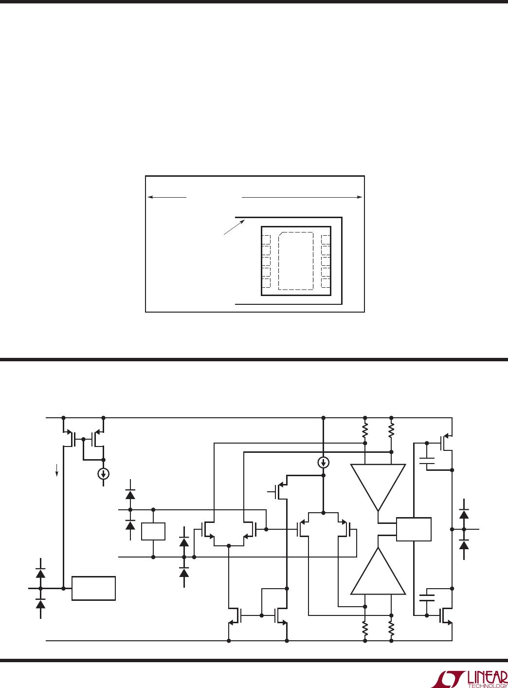
–15
PERCENTAGE OF UNITS
0.30
0.25
0.20
0.15
0.10
0.5
0
60812 F01
–12 –9 –3–6 0
V
OS
CHANGE (µV)
151293 6
V
OS
CHANGE AFTER 3 THERMAL CYCLES
V
CM
= 0.5V
V
+
= 3V
300 UNITS
applicaTions inForMaTion
Preserving Input Precision
Preserving input accuracy of the LTC6081/LTC6082 re-
quires that the application circuit and PC board layout do
not introduce errors comparable or greater than the 5µ
V
typical offset of the amplifiers. T
emperature differentials
across the input connections can generate thermocouple
voltages of 10’s of microvolts so the connections to the
input leads should be short, close together and away from
heat dissipating components. Air current across the board
can also generate temperature differentials.
The extremely low input bias currents (0.1pA typical) al
-
low high accuracy to be maintained with high impedance
sources and feedback resistors. Leakage currents on the
PC board can be higher than the input bias current. For
example, 10GΩ of leakage between a 5V supply lead and
an input lead will generate 500pA! Surround the input
leads with a guard ring driven to the same potential as the
input common mode voltage to avoid excessive leakage
in high impedance applications.
Capacitive Load
LTC6081/LTC6082 can drive capacitive load up to 200pF in
unity gain. The capacitive load driving capability increases
as the amplifier is used in higher gain configurations. A
small series resistance between the output and the load
further increases the amount of capacitance the amplifier
can drive.
SHDN Pins
Pins 5 and 6 are used for power shutdown on the LTC6081
in the DD package. If they are floating, internal current
sources pull Pins 5 and 6 to V
+
and the amplifiers operate
normally. In shutdown, the amplifier output is high im-
pedance, and each amplifier draws less than 2µA current.
Rail-to-Rail Input
The input stage of L
TC6081/L
TC6082 combines both PMOS
and NMOS differential pairs, extending its input common
mode voltage range to both positive and negative supply
voltages. At high input common mode range, the NMOS
pair is on. At low common mode range, the PMOS pair is
on. The transition happens when the common voltage is
between 1.3V and 0.9V below the positive supply. LTC6081
has better low frequency noise performance with PMOS
input on due to its lower flicker noise (see Voltage Noise
vs Frequency and 0.1Hz to 10Hz Input Voltage Noise in
Typical Performance Characteristics).
Thermal Hysteresis
Figure 1 shows the input offset voltage hysteresis of the
LTC6081IMS8 for 3 thermal cycles from –45°C to 90°C.
The typical offset shift is ±4µV. The data was taken with
the ICs in stress free sockets. Mounting to PC boards
may cause additional hysteresis due to mechanical stress.
The LTC6081 will meet offset voltage specifications in the
electrical characteristics table even after 15µV of additional
error from thermal hysteresis.
Figure 1. V
OS
Thermal Hysteresis of LTC6081MS8