LTC6081/LTC6082
6
60812fd
For more information www.linear.com/LTC6081
The ● denotes the specifications which apply over the full operating
temperature range, otherwise specifications are at T
A
= 25°C. Test conditions are V
+
= 5V, V
–
= 0V, V
CM
= 0.5V unless otherwise noted.
Note 1: Stresses beyond those listed under Absolute Maximum Ratings
may cause permanent damage to the device. Exposure to any Absolute
Maximum Rating condition for extended periods may affect device
reliability and lifetime.
Note 2: A heat sink may be required to keep the junction temperature
below the absolute maximum. This depends on the power supply voltage
and how many amplifiers are shorted.
Note 3: The LTC6081C/LTC6082C and LTC6081I/LTC6082I are guaranteed
functional over the operating temperature range of –40°C to 85°C.
The LTC6081H/LTC6082H are guaranteed functional over the operating
temperature range of –40°C to 125°C.
Note 4: The LTC6081C/LTC6082C are guaranteed to meet specified
performance from 0°C to 70°C. The LTC6081C/LTC6082C are designed,
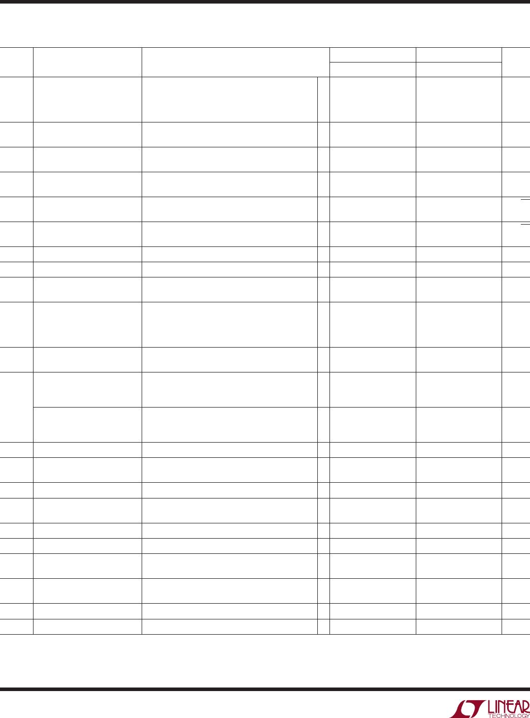
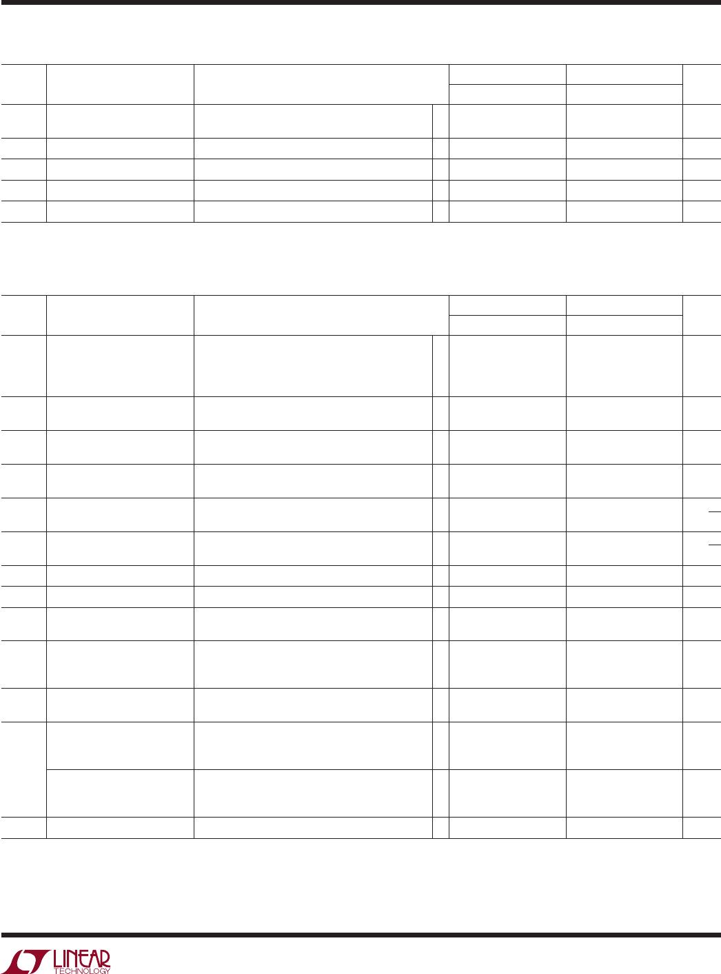
elecTrical characTerisTics
SYMBOL PARAMETER CONDITIONS
C, I SUFFIXES H SUFFIX
UNITSMIN TYP MAX MIN TYP MAX
I
SC
Output Short-Circuit Current Source
Sink
●
●
24
24
21
21
mA
mA
SR Slew Rate A
V
= 1 1 1 V/μs
GBW Gain-Bandwidth Product
(f
TEST
= 50kHz)
R
L
= 100k
●
2.5
1.8
3.5 2.5
1.5
3.5 MHz
MHz
F
0
Phase Margin R
L
= 10k 70 70 Deg
t
S
Settling Time 0.1% A
V
= 1, 1V Step 6 6 μs
I
S
Supply Current
(Per Amplifier)
No Load
●
340 425
465
340 425
490
μA
μA
Shutdown Current
(Per Amplifier)
Shutdown, V
SHDN
≤ 1.2V
●
6 μA
V
S
Supply Voltage Range Guaranteed by the PSRR Test
●
2.7 5.5 2.7 5.5 V
Channel Separation f
s
= 10kHz, R
L
= 10k –120 –120 dB
Shutdown Logic SHDN High
SHDN Low
●
●
3.5
1.2
3.5
1.2
V
V
THD Total Harmonic Distortion
f = 10kHz, V
+
= 5V, V
OUT
= 2V
P-P
, R
L
= 10k –90 –90 dB
t
ON
Turn-On Time V
SHDN
= 1.2V to 3.5V 10 10 µs
t
OFF
Turn-Off Time V
SHDN
= 3.5V to 1.2V 2 2 µs
SHDN Pin Current V
SHDN
= 0V
●
2 μA
characterized and expected to meet specified performance from –40°C
to 85°C but are not tested or QA sampled at these temperatures. The
LTC6081I/LTC6082I are guaranteed to meet specified performance from
–40°C to 85°C. The LTC6081H/LTC6082H are guaranteed to meet specified
performance from –40°C to 125°C.
Note 5: Input offset drift is computed from the limits of the V
OS
test
divided by the temperature range. This is a conservative estimate of worst
case drift. Consult the Typical Performance Characteristics section for
more information on input offset drift.
Note 6: I
B
guaranteed by the V
S
= 5V test.
Note 7: Current noise is calculated from I
n
= √2qI
B
, where q = 1.6 • 10
–19
coulomb.
Note 8: V
OS
drift is guaranteed by the V
S
= 3V test.