SM6S33ATHE3/I

SM6S10AT thru SM6S43AT
www.vishay.com
Vishay General Semiconductor
Revision: 09-Apr-15
1
Document Number: 87735
For technical questions within your region: DiodesAmericas@vishay.com
, DiodesAsia@vishay.com, DiodesEurope@vishay.com
THIS DOCUMENT IS SUBJECT TO CHANGE WITHOUT NOTICE. THE PRODUCTS DESCRIBED HEREIN AND THIS DOCUMENT
ARE SUBJECT TO SPECIFIC DISCLAIMERS, SET FORTH AT www.vishay.com/doc?91000
Surface Mount PAR
®
Transient Voltage Suppressors
High Temperature Stability and High Reliability Conditions
FEATURES
Junction passivation optimized design passivated
anisotropic rectifier technology
•T
J
= 175 °C capability suitable for high reliability
and automotive requirement
Available in uni-directional polarity only
Low leakage current
Low forward voltage drop
High surge capability
Meets ISO7637-2 surge specification (varied by test
condition)
Meets MSL level 1, per J-STD-020, LF maximum peak
of 245 °C
AEC-Q101 qualified
- Automotive ordering code: base P/NHE3
Material categorization: for definitions of compliance
please see www.vishay.com/doc?99912
TYPICAL APPLICATIONS
Use in sensitive electronics protection against voltage
transients induced by inductive load switching and lighting,
especially for automotive load dump protection application.
MECHANICAL DATA
Case: DO-218AC
Molding compound meets UL 94 V-0 flammability rating
Base P/NHE3 - RoHS-compliant, AEC-Q101 qualified
Terminals: Matte tin plated leads, solderable per
J-STD-002 and JESD 22-B102
HE3 suffix meets JESD 201 class 2 whisker test
Polarity: Heatsink is anode
Note
(1)
Non-repetitive current pulse at T
A
= 25 °C
PRIMARY CHARACTERISTICS
V
WM
10 V to 43 V
V
BR
11.1 V to 52.8 V
P
PPM
(10 x 1000 μs) 4600 W
P
PPM
(10 x 10 000 μs) 3600 W
P
D
6 W
I
FSM
600 A
T
J
max. 175 °C
Polarity Uni-directional
Package DO-218AC
DO-218 Compatible
MAXIMUM RATINGS (T
C
= 25 °C unless otherwise noted)
PARAMETER SYMBOL VALUE UNIT
Peak pulse power dissipation
with 10/1000 μs waveform
P
PPM
4600
W
with 10/10 000 μs waveform 3600
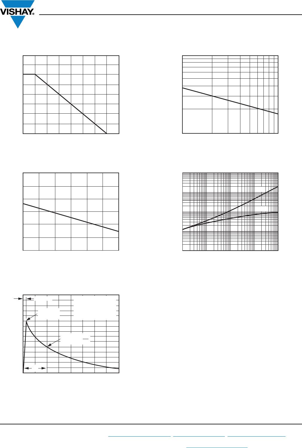
Power dissipation on infinite heatsink at T
C
= 25 °C (fig. 1) P
D
6.0 W
Peak pulse current with 10/1000 μs waveform I
PPM
(1)
See next table A
Peak forward surge current 8.3 ms single half sine-wave I
FSM
600 A
Operating junction and storage temperature range T
J
, T
STG
-55 to +175 °C
SM6S10AT thru SM6S43AT
www.vishay.com
Vishay General Semiconductor
Revision: 09-Apr-15
2
Document Number: 87735
For technical questions within your region: DiodesAmericas@vishay.com
, DiodesAsia@vishay.com, DiodesEurope@vishay.com
THIS DOCUMENT IS SUBJECT TO CHANGE WITHOUT NOTICE. THE PRODUCTS DESCRIBED HEREIN AND THIS DOCUMENT
ARE SUBJECT TO SPECIFIC DISCLAIMERS, SET FORTH AT www.vishay.com/doc?91000
Note
For all types maximum V
F
= 1.9 V at I
F
= 100 A measured on 8.3 ms single half sine-wave or equivalent square wave, duty cycle = 4 pulses
per minute maximum
Note
(1)
AEC-Q101 qualified
ELECTRICAL CHARACTERISTICS (T
C
= 25 °C unless otherwise noted)
DEVICE
TYPE
BREAKDOWN
VOLTAGE
V
BR
(V)
TEST
CURRENT
I
T
(mA)
STAND-OFF
VOLTAGE
V
WM
(V)
MAXIMUM
REVERSE
LEAKAGE
AT V
WM
I
D
(μA)
MAXIMUM REVERSE
LEAKAGE
AT V
WM
T
J
= 175 °C
I
D
(μA)
MAX. PEAK
PULSE CURRENT
AT 10/1000 μs
WAVEFORM
(A)
MAXIMUM
CLAMPING
VOLTAGE
AT I
PPM
V
C
(V)
MIN. MAX.
SM6S10AT 11.1 12.3 5.0 10.0 15 250 271 17.0
SM6S11AT 12.2 13.5 5.0 11.0 10 150 253 18.2
SM6S12AT 13.3 14.7 5.0 12.0 10 150 231 19.9
SM6S13AT 14.4 15.9 5.0 13.0 10 150 214 21.5
SM6S14AT 15.6 17.2 5.0 14.0 10 150 198 23.2
SM6S15AT 16.7 18.5 5.0 15.0 10 150 189 24.4
SM6S16AT 17.8 19.7 5.0 16.0 10 150 177 26.0
SM6S17AT 18.9 20.9 5.0 17.0 10 150 167 27.6
SM6S18AT 20.0 22.1 5.0 18.0 10 150 158 29.2
SM6S20AT 22.2 24.5 5.0 20.0 10 150 142 32.4
SM6S22AT 24.4 26.9 5.0 22.0 10 150 130 35.5
SM6S24AT 26.7 29.5 5.0 24.0 10 150 118 38.9
SM6S26AT 28.9 31.9 5.0 26.0 10 150 109 42.1
SM6S28AT 31.1 34.4 5.0 28.0 10 150 101 45.4
SM6S30AT 33.3 36.8 5.0 30.0 10 150 95 48.4
SM6S33AT 36.7 40.6 5.0 33.0 10 150 86 53.3
SM6S36AT 40.0 44.2 5.0 36.0 10 150 79 58.1
SM6S40AT 44.4 49.1 5.0 40.0 10 150 71 64.5
SM6S43AT 47.8 52.8 5.0 43.0 10 150 66 69.4
THERMAL CHARACTERISTICS (T
C
= 25 °C unless otherwise noted)
PARAMETER SYMBOL VALUE UNIT
Typical thermal resistance, junction to case R
JC
0.95 °C/W
ORDERING INFORMATION (Example)
PREFERRED P/N UNIT WEIGHT (g) PREFERRED PACKAGE CODE BASE QUANTITY DELIVERY MODE
SM6S10ATHE3/I
(1)
2.550 I 750
13" diameter plastic tape and reel,
anode towards the sprocket hole
SM6S10AT thru SM6S43AT
www.vishay.com
Vishay General Semiconductor
Revision: 09-Apr-15
3
Document Number: 87735
For technical questions within your region: DiodesAmericas@vishay.com
, DiodesAsia@vishay.com, DiodesEurope@vishay.com
THIS DOCUMENT IS SUBJECT TO CHANGE WITHOUT NOTICE. THE PRODUCTS DESCRIBED HEREIN AND THIS DOCUMENT
ARE SUBJECT TO SPECIFIC DISCLAIMERS, SET FORTH AT www.vishay.com/doc?91000
RATINGS AND CHARACTERISTICS CURVES (T
A
= 25 °C unless otherwise noted)
Fig. 1 - Power Derating Curve
Fig. 2 - Load Dump Power Characteristics
(10 ms Exponential Waveform)
Fig. 3 - Pulse Waveform
Fig. 4 - Reverse Power Capability
Fig. 5 - Typical Transient Thermal Impedance
0
2.0
4.0
6.0
8.0
0
50
100
150 200
Power Dissipation (W)
Case Temperature (°C)
0
2000
1000
3000
4000
5000
6000
25
50 75
100 125
150 175
Load Dump Power (W)
Case Temperature (°C)
0
50
100
150
0
1.0
2.0
3.0 4.0
Input Peak Pulse Current (%)
t - Time (ms)
t
d
t
r
= 10 μs
Peak Value
I
PPM
Half Value -
I
PPM
I
PP
2
T
J
= 25 °C
Pulse Width (t
d
) is
Dened as the Point
Where the Peak Current
Decays to 50 % of I
PPM
Reverse Surge Power (W)
1000
10 000
10
100
Pulse Width (ms) - ½ I
PP
Exponential Waveform
t - Pul
se Width (s)
Transient Thermal Impedance (°C/W)
100
10
1
0.1
0.01
0.01 0.1 1 10 100
R
θJC
R
θJA

SM6S33ATHE3/I

Mfr. #:
Manufacturer:
Vishay Semiconductors
Description:
TVS Diodes / ESD Suppressors 6W,33V 5%,SMD PAR
Lifecycle:
New from this manufacturer.
Delivery:
DHL FedEx Ups TNT EMS
Payment:
T/T Paypal Visa MoneyGram Western Union