23S05-1HDCGI8

4
COMMERCIAL AND INDUSTRIAL TEMPERATURE RANGES
IDT23S05
3.3V ZERO DELAY CLOCK BUFFER, SPREAD SPECTRUM
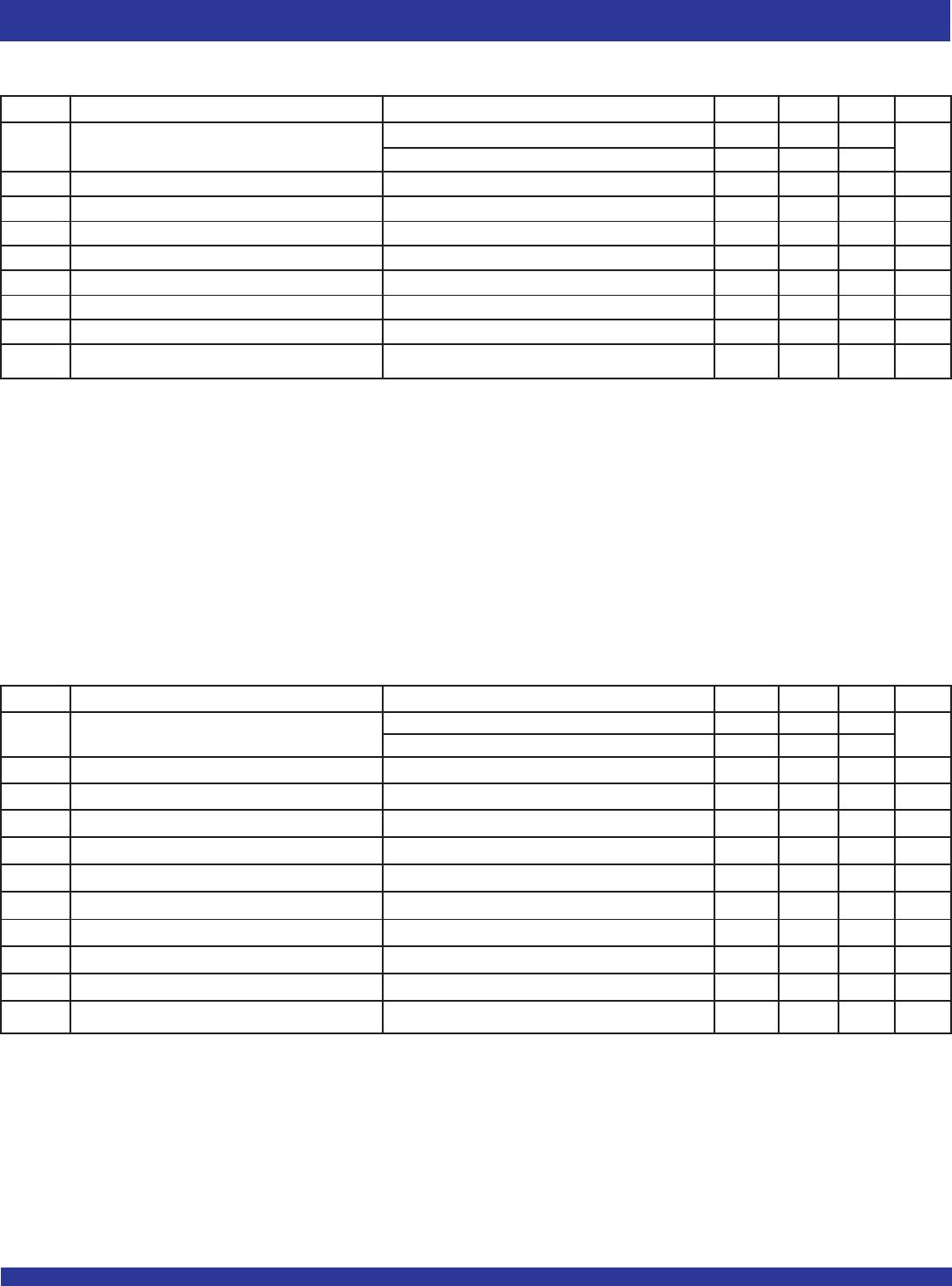
Symbol Parameter Min. Max. Unit
VDD Supply Voltage 3 3.6 V
TA Operating Temperature (Ambient Temperature) -40 +85 ° C
CL Load Capacitance < 100MHz 30 pF
Load Capacitance 100MHz - 133MHz 10
CIN Input Capacitance 7 pF
OPERATING CONDITIONS - INDUSTRIAL
SWITCHING CHARACTERISTICS (23S05-1H) - COMMERCIAL
(1,2)
Symbol Parameter Conditions Min. Typ. Max. Unit
t1 Output Frequency 10pF Load 10 133 MHz
30pF Load 10 100
Duty Cycle = t2 ÷ t1 Measured at 1.4V, FOUT = 66.66MHz 40 50 60 %
Duty Cycle = t2 ÷ t1 Measured at 1.4V, FOUT <50MHz 45 50 55 %
t3 Rise Time Measured between 0.8V and 2V 1.5 ns
t4 Fall Time Measured between 0.8V and 2V 1.5 ns
t5 Output to Output Skew All outputs equally loaded 250 ps
t6 Delay, REF Rising Edge to CLKOUT Rising Edge Measured at VDD/2 0 ±350 ps
t7 Device-to-Device Skew Measured at VDD/2 on the CLKOUT pins of devices 0 700 ps
t8 Output Slew Rate Measured between 0.8V and 2V using Test Circuit #2 1 V/ns
tJ Cycle-to-Cycle Jitter, pk - pk Measured at 66.66MHz, loaded outputs 200 ps
tLOCK PLL Lock Time Stable power supply, valid clock presented on REF pin 1 ms
NOTES:
1. REF Input has a threshold voltage of VDD/2.
2. All parameters specified with loaded outputs.
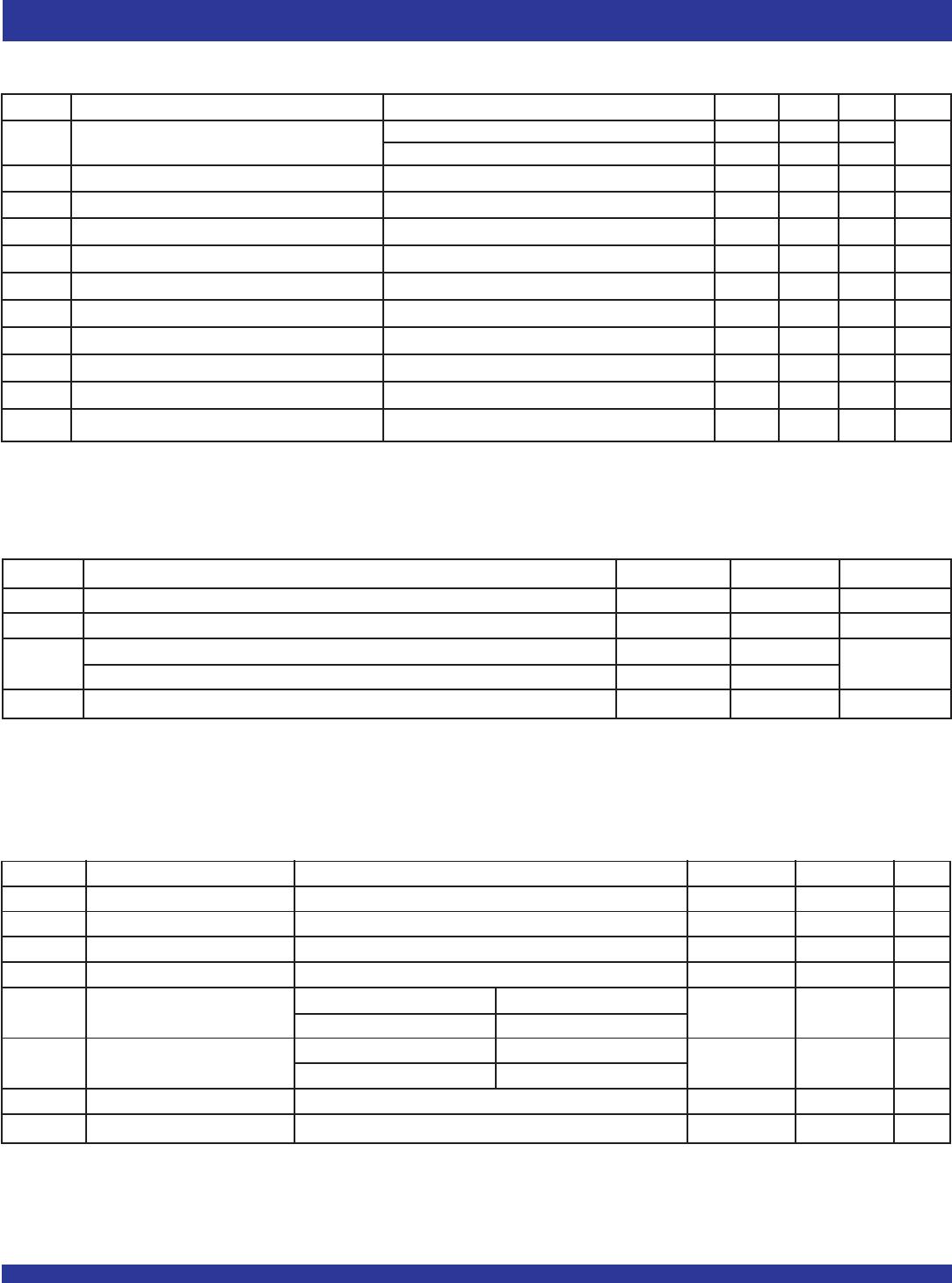
DC ELECTRICAL CHARACTERISTICS - INDUSTRIAL
Symbol Parameter Conditions Min. Max. Unit
VIL Input LOW Voltage Level 0.8 V
VIH Input HIGH Voltage Level 2 V
IIL Input LOW Current VIN = 0V 50 µA
IIH Input HIGH Current VIN = VDD 100 µA
VOL Output LOW Voltage Standard Drive IOL = 8mA 0.4 V
High Drive IOL = 12mA (-1H)
VOH Output HIGH Voltage Standard Drive IOH = -8mA 2.4 V
High Drive IOH = -12mA (-1H)
IDD_PD Power Down Current REF = 0MHz 25 µA
IDD Supply Current Unloaded Outputs at 66.66MHz 35 mA
5
COMMERCIAL AND INDUSTRIAL TEMPERATURE RANGES
IDT23S05
3.3V ZERO DELAY CLOCK BUFFER, SPREAD SPECTRUM
SWITCHING CHARACTERISTICS (23S05-1H) - INDUSTRIAL
(1,2)
Symbol Parameter Conditions Min. Typ. Max. Unit
t1 Output Frequency 10pF Load 10 133 MHz
30pF Load 10 100
Duty Cycle = t2 ÷ t1 Measured at 1.4V, FOUT = 66.66MHz 40 50 60 %
Duty Cycle = t2 ÷ t1 Measured at 1.4V, FOUT <50MHz 45 50 55 %
t3 Rise Time Measured between 0.8V and 2V 1.5 ns
t4 Fall Time Measured between 0.8V and 2V 1.5 ns
t5 Output to Output Skew All outputs equally loaded 250 ps
t6 Delay, REF Rising Edge to CLKOUT Rising Edge Measured at VDD/2 0 ±350 ps
t7 Device-to-Device Skew Measured at VDD/2 on the CLKOUT pins of devices 0 700 ps
t8 Output Slew Rate Measured between 0.8V and 2V using Test Circuit #2 1 V/ns
tJ Cycle-to-Cycle Jitter, pk - pk Measured at 66.66MHz, loaded outputs 200 ps
tLOCK PLL Lock Time Stable power supply, valid clock presented on REF pin 1 ms
NOTES:
1. REF Input has a threshold voltage of VDD/2.
2. All parameters specified with loaded outputs.
SWITCHING CHARACTERISTICS (23S05-1) - INDUSTRIAL
(1,2)
Symbol Parameter Conditions Min. Typ. Max. Unit
t1 Output Frequency 10pF Load 10 133 MHz
30pF Load 10 100
Duty Cycle = t2 ÷ t1 Measured at 1.4V, FOUT = 66.66MHz 40 50 60 %
t3 Rise Time Measured between 0.8V and 2V 2.5 ns
t4 Fall Time Measured between 0.8V and 2V 2.5 ns
t5 Output to Output Skew All outputs equally loaded 250 ps
t6 Delay, REF Rising Edge to CLKOUT Rising Edge Measured at VDD/2 0 ±350 ps
t7 Device-to-Device Skew Measured at VDD/2 on the CLKOUT pins of devices 0 700 ps
tJ Cycle-to-Cycle Jitter, pk - pk Measured at 66.66MHz, loaded outputs 200 ps
tLOCK PLL Lock Time Stable power supply, valid clock presented on REF pin 1 ms
NOTES:
1. REF Input has a threshold voltage of VDD/2.
2. All parameters specified with loaded outputs.
6
COMMERCIAL AND INDUSTRIAL TEMPERATURE RANGES
IDT23S05
3.3V ZERO DELAY CLOCK BUFFER, SPREAD SPECTRUM
ZERO DELAY AND SKEW CONTROL
All outputs should be uniformly loaded in order to achieve Zero I/O Delay. Since the CLKOUT pin is the internal feedback for the PLL, its relative
loading can affect and adjust the input/output delay.
For designs utilizing zero I/O Delay, all outputs including CLKOUT must be equally loaded. Even if the output is not used, it must have a capacitive
load equal to that on the other outputs in order to obtain true zero I/O Delay. If I/O Delay adjustments are needed, use the Output Load Difference diagram
to calculate loading differences between the CLKOUT pin and other outputs. For zero output-to-output skew, all outputs must be loaded equally.
SPREAD SPECTRUM COMPATIBLE
Many systems being designed now use a technology called Spread Spectrum Frequency Timing Generation. This product is designed not to filter
off the Spread Spectrum feature of the reference input, assuming it exists. When a zero delay buffer is not designed to pass the Spread Spectrum feature
through, the result is a significant amount of tracking skew, which may cause problems in systems requiring synchronization.

23S05-1HDCGI8

Mfr. #:
Manufacturer:
IDT
Description:
Clock Buffer 3.3V CLOCK BUFFER SPREAD SPECTRUM
Lifecycle:
New from this manufacturer.
Delivery:
DHL FedEx Ups TNT EMS
Payment:
T/T Paypal Visa MoneyGram Western Union