REV.
SSM2019
–3–
ABSOLUTE MAXIMUM RATINGS
1
Supply Voltage . . . . . . . . . . . . . . . . . . . . . . . . . . . . . . . . ± 19 V
Input Voltage . . . . . . . . . . . . . . . . . . . . . . . . . . Supply Voltage
Output Short Circuit Duration . . . . . . . . . . . . . . . . . . . 10 sec
Storage Temperature Range . . . . . . . . . . . . –65∞C to +150∞C
Junction Temperature (T
J
) . . . . . . . . . . . . . –65∞C to +150∞C
Lead Temperature Range (Soldering, 60 sec) . . . . . . . . 300∞C
Operating Temperature Range . . . . . . . . . . . –40∞C to +85∞C
Thermal Resistance
2
8-Lead PDIP (N) . . . . . . . . . . . . . . . . . . . . . . .
JA
= 96∞C/W
. . . . . . . . . . . . . . . . . . . . . . . . . . . . . . . . . . . . .
JC
= 37∞C/W
16-Lead SOIC (RW) . . . . . . . . . . . . . . . . . . . .
JA
= 92∞C/W
. . . . . . . . . . . . . . . . . . . . . . . . . . . . . . . . . . . . .
JC
= 27∞C/W
NOTES
1
Stresses above those listed under Absolute Maximum Ratings may cause perma-
nent damage to the device. This is a stress rating only; functional operation of the
device at these or any other conditions above those indicated in the operational
section of this specification is not implied. Exposure to absolute maximum rating
conditions for extended periods may affect device reliability.
2
q
JA
is specified for worst-case mounting conditions, i.e., q
JA
is specified for device
in socket for PDIP; q
JA
is specified for device soldered to printed circuit board for
SOIC package.
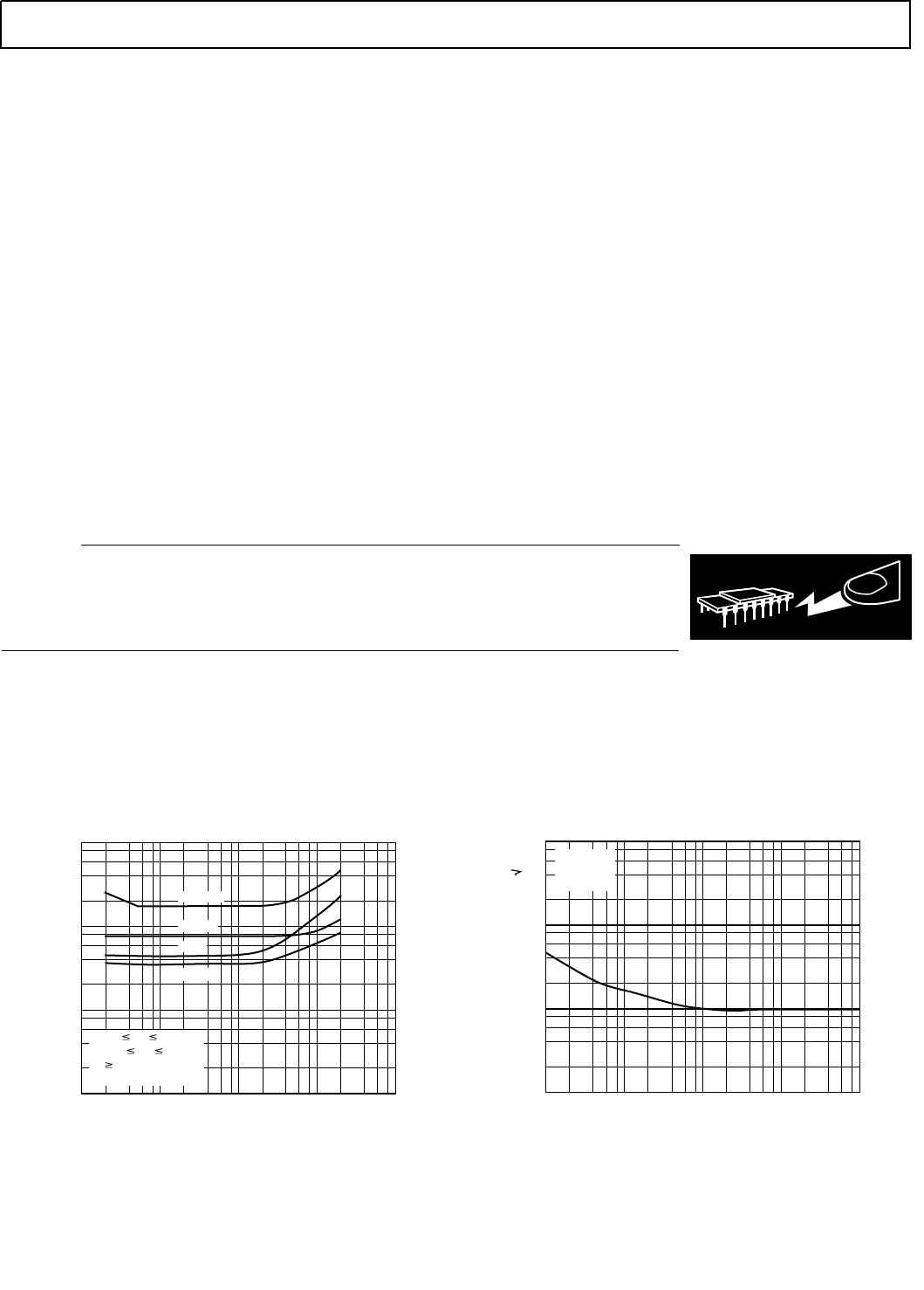
FREQUENCY – Hz
THD + N – %
0.0001
10
0.001
0.01
0.1
20 100 1k 10k 20k
ⴞ15V V
S
ⴞ18V
7Vrms
V
O
10Vrms
R
L
600⍀
BW = 80kHz
G = 10
G = 1000
G = 100
G = 1
TPC 1. Typical THD + Noise vs. Gain
FREQUENCY – Hz
RTI, VOLTAGE NOISE DENSITY – nV/ Hz
0.1
110100 1k 10k
1
10
100
T
A
= 25ⴗC
V
S
= ⴞ15V
G = 1000
TPC 2. Voltage Noise Density vs. Frequency
WARNING!
ESD SENSITIVE DEVICE
CAUTION
ESD (electrostatic discharge) sensitive device. Electrostatic charges as high as 4000 V readily
accumulate on the human body and test equipment and can discharge without detection. Although
the SSM2019 features proprietary ESD protection circuitry, permanent damage may occur on
devices subjected to high energy electrostatic discharges. Therefore, proper ESD precautions are
recommended to avoid performance degradation or loss of functionality.
Typical Performance Characteristics